Thin film used for hole sealing of porous interconnection dielectric surface and preparing method of thin film

A dielectric surface and thin film technology, applied in the fields of semiconductor/solid-state device manufacturing, electrical components, electrical solid-state devices, etc., can solve the problem of the decrease in the adhesion of the cap layer, the increase in the effective dielectric constant of the interconnect dielectric layer, the mechanical properties and electrical properties. problems such as drop, to achieve the effects of excellent uniformity, excellent mechanical properties, and excellent insulation properties

Inactive Publication Date: 2014-07-30
FUDAN UNIV
View PDF5 Cites 2 Cited by
  • Summary
  • Abstract
  • Description
  • Claims
  • Application Information

AI Technical Summary

Problems solved by technology

Using PECVD technology, doping porogens in organic liquid sources can effectively reduce the dielectric constant, but its mechanical properties and electrical properties will decrease
On the other hand, because the ultra-low-k material has the characteristics of high porosity, it will cause its adhesion to the capping layer to decrease, or more capping layer material will enter the pores of the ultra-low-k material, resulting in the effective interconnection of the dielectric layer. Increased dielectric constant

Method used


Image

  • Thin film used for hole sealing of porous interconnection dielectric surface and preparing method of thin film
  • Thin film used for hole sealing of porous interconnection dielectric surface and preparing method of thin film

Examples


Embodiment Construction

[0025] 1. Put a wafer covered with a low dielectric constant (k) porous interconnection medium on a tray in the reaction chamber of a plasma-enhanced chemical vapor deposition (PECVD) device. The porous material is a porous SiCOH film, or Porous SiO 2 film. Close the cavity, and then evacuate the cavity to 0.02-0.03 torr.

[0026] 2. Raise the temperature of the substrate to 200-400 °C, and then inject He gas to preheat the gas pipeline to prevent the incompletely vaporized liquid source from condensing on the tube wall.

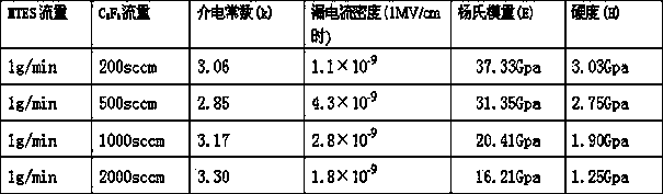
[0027] 3. Through the control of LFM, MTES is fed into the vaporizer at a fixed flow rate of 1g / min, and the vaporized MTES is loaded into the reaction chamber through He gas, and the flow rate of the carrier gas He is 5000 sccm.

[0028] 4. Another reaction gas C 2 f 6 It is controlled directly into the reaction chamber by a mass flow meter (MFC), and its flow rate is 200-2000 sccm.

[0029] 5. In the reaction chamber, C 2 f 6 Mix with vaporized MTES...


PUM

PropertyMeasurementUnit
current densityaaaaaaaaaa
electrical resistivityaaaaaaaaaa
hardnessaaaaaaaaaa

Abstract

The invention belongs to the technical field of super-large-scale integrated circuits, and particularly relates to a method for preparing a material for hole sealing of a porous interconnection dielectric surface. An organic liquid state source MTES is taken as a liquid source and enters a cavity along with He carrier gas after being vaporized to be mixed with C2F6 gas, a plasma enhanced chemical vapor deposition (PECVD) process is adopted, and a thin film is deposited on the porous low-dielectric-constant interconnection dielectric surface. The dielectric constant of the thin film is 2.8-3.3, the order of magnitude of the leakage current density is 10-9 A / cm2 under the electric field strength of 1 MV / cm, the Young modulus is 16.21-37.33 GPa, and the hardness is 1.25-3.03 GPa. The thin film can be used for hole sealing of the porous interconnection dielectric surface in super-large-scale integrated circuit rear-end interconnection, and meanwhile performs the function of improving adhesion strength between a porous dielectric layer and a cap layer or a diffusion impervious layer.

Description

technical field [0001] The invention belongs to the technical field of ultra-large-scale integrated circuit manufacturing, and in particular relates to a film used for sealing pores on the surface of a porous interconnection medium and a preparation method thereof. Background technique [0002] Due to the large-scale development of integrated circuits, its feature size has also decreased rapidly, which has led to a sharp increase in the delay of integrated circuit interconnection RC (R refers to resistance, C refers to capacitance), which greatly limits the speed of circuit operation, and It brings the problems of signal crosstalk and increased power consumption. Replacing aluminum with copper can reduce the resistance of integrated circuits; similarly, reducing parasitic capacitance is also an effective way to improve the performance of integrated circuits. Among them, replacing SiO with low dielectric constant (k) materials 2 (k≈4.0) is an effective method [1]. In order ...

Claims


Application Information

Patent Timeline
Patent Type & Authority Applications(China)
IPC IPC(8): H01L21/768H01L23/522
CPCH01L21/7682H01L23/5329H01L2221/1047
Inventor 丁士进黄毅华张卫
Owner FUDAN UNIV
Why Eureka
Try Eureka