Preparation process of molybdenum carbide-doped ruthenium-based alloy diffusion barrier layer for copper-free seed crystal interconnection

A ruthenium-based alloy and preparation process technology, applied in the field of preparation of new diffusion barrier layers, to achieve the effects of less pollutants, low cost, and strong oxidation resistance

Inactive Publication Date: 2016-09-07
SICHUAN UNIV
View PDF4 Cites 0 Cited by
  • Summary
  • Abstract
  • Description
  • Claims
  • Application Information

AI Technical Summary

Problems solved by technology

The remaining Mo and Ta doped Ru alloys also have recrystallization at higher temperatures. Therefore, the performance of ultra-thin (<5 nm) Ru-based alloy barrier layers with high thermal stability faces great challenges.

Method used


Image

  • Preparation process of molybdenum carbide-doped ruthenium-based alloy diffusion barrier layer for copper-free seed crystal interconnection
  • Preparation process of molybdenum carbide-doped ruthenium-based alloy diffusion barrier layer for copper-free seed crystal interconnection

Examples


Embodiment 1

[0029] The molybdenum carbide-doped ruthenium-based alloy (RuMoC) barrier layer preparation process used in this embodiment includes the following steps:

[0030] a. Clean the substrate material:

[0031] Put the monocrystalline silicon (Si) / carbon-doped silicon oxide (SiOC:H, 200 nm) multi-layer structure substrate material into acetone and absolute ethanol for 20 minutes for ultrasonic cleaning respectively, and put it into a vacuum chamber after drying. Then evacuate to 2.0×10 -4 Pa;

[0032] b. Treatment of the substrate before deposition: bias backsputtering;

[0033] Under the vacuum condition of step a, the Si / SiOC:H substrate was cleaned by bias backsputtering for 5 minutes to remove impurities on the surface of the Si / SiOC:H substrate, the backsputter power was 100 W, and the backsputter bias was -500 V ; The backsplash gas is argon (Ar); the working vacuum is 1.0 Pa;

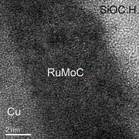
[0034] c. Deposition of RuMoC barrier film:

[0035] Using reactive magnetron sputtering tech...

Embodiment 2、3

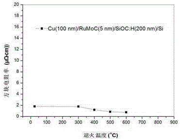
[0039] During the deposition of the RuMoC barrier layer, the deposition bias and sputtering power have an impact on the composition, uniformity and thickness of the coating. The operating steps, conditions and parameters of the RuMoC barrier layer in this example are basically the same as those in Example 1. Only by changing the deposition bias or sputtering power of the magnetron Ru target and the magnetron MoC target when depositing the RuMoC barrier layer, for example, the selected deposition bias is -50 V, -100 V, -150 V, -200 V , or the sputtering power is 50 W, 100 W, 150 W, 200 W, the composition, uniformity and thickness of the RuMoC barrier layer can be adjusted, and then the thickness, resistivity and high temperature resistance of the RuMoC barrier layer can be adjusted. , to meet the usage requirements of the product.

Embodiment 4

[0041] Because in the process of depositing the RuMoC barrier layer, the content of C has a great influence on the composition, structure and electrical properties of the barrier layer. The operating steps, conditions and parameters of the RuMoC barrier layer in this example are basically the same as those in Example 1. Only by changing the magnetron MoC target power to change the content of C and Mo when depositing the barrier layer of RuMoC barrier layer to change the coating structure and composition, such as the selected magnetron MoC target power is 50 W, 100 W, 150 W, 200 W, and then adjusting the percentage of Ge atoms in the range of 6.5, 12.5, 17.5, 25 (%) can control the composition and structure of the RuMoC barrier layer, and then realize the thickness, resistivity and high temperature resistance of the RuMoC barrier layer, etc. The performance is adjusted to meet the usage needs of the product application.

[0042] The used substrate material of the present inven...


PUM

PropertyMeasurementUnit
electrical resistivityaaaaaaaaaa

Abstract

The invention discloses a preparation technology of a molybdenum-carbide-doped ruthenium-base alloy (RuMoC) diffusion barrier layer, and relates to a novel preparation technology of a diffusion impervious layer between copper (Cu) and a silicon-oxide-based insulating medium (SiOC: H) in an ultra-deep submicron integrated circuit back-end interconnection structure. The thermal stable temperature of the RuMoC (5 nm) barrier layer deposited through the preparation technology can reach above 600 DEG C, and the situation that copper atoms diffuse towards the inner portion of a silicon-oxide-based medium body can be restrained effectively. The RuMoC (5 nm) barrier layer prepared through the technology can effectively reduce the electrical resistivity of an interconnection film system, reduce the resistance-capacitance coupling (RC) delay effect of interconnection circuits, increase the operating speed of semiconductor devices and improve the stability of the semiconductor devices.

Description

technical field [0001] The invention belongs to the technical field of semiconductor integrated circuit manufacturing technology, and relates to copper (Cu) and low dielectric constant (low dielectric constant) in the back-end interconnection of ultra-deep submicron integrated circuits. -k ) preparation process of a novel diffusion barrier layer between silicon oxide-based insulating dielectrics (SiOC:H). Background technique [0002] Today, copper (Cu) interconnection materials and low dielectric constant (low -k ) to replace traditional Al / SiO 2 structure to deal with the sharply increased resistance-capacitance ( RC ) delay and power dissipation effects. Since Cu is easily oxidized and easily interacts with silicon oxide-based oxide dielectrics (low -k ) reaction to form deep-level impurities, which have a strong trap effect on carriers, degrading or even failing device performance, see literature [B. Liu, Z.X. Song, Y.H. Li, K.W. Xu, Appl. Phys. Lett. 93 / 17 (2008)]...

Claims


Application Information

Patent Timeline
Patent Type & Authority Patents(China)
IPC IPC(8): H01L21/768H01L21/3205
CPCH01L21/76885
Inventor 刘波张彦坡林黎蔚廖小东
Owner SICHUAN UNIV
Why Eureka
Try Eureka