MEMS aluminum and germanium bonding structure and manufacturing method thereof

A technology of aluminum-germanium bonding and manufacturing method, which is applied in the field of MEMS, can solve problems such as easy extension and flow of aluminum-germanium, low production efficiency at bonding temperature, and overall performance of devices destroyed, so as to optimize bonding quality and increase effective tube The number of cores and the effect of reducing the layout area

Active Publication Date: 2014-08-13
HANGZHOU SILAN INTEGRATED CIRCUIT
View PDF7 Cites 22 Cited by
  • Summary
  • Abstract
  • Description
  • Claims
  • Application Information

AI Technical Summary

Problems solved by technology

[0004] In these bonding processes, compared with other bonding processes, AlGe eutectic bonding has the advantages of low bonding temperature, good sealing effect, high bonding strength, high production efficiency, low cost, and can Compatible with CMOS technology, so it is widely used in wafer-level packaging of MEMS products; the disadvantage is that during the bonding and sintering process, AlGe is prone to extension and flow, and the extended part of AlGe may affect the movable structure of MEMS micromachines. Work, so that the device is destroyed or the overall performance is reduced, and the extension and flow of aluminum germanium leads to the need to occupy a large bonding area

Method used


Image

  • MEMS aluminum and germanium bonding structure and manufacturing method thereof
  • MEMS aluminum and germanium bonding structure and manufacturing method thereof
  • MEMS aluminum and germanium bonding structure and manufacturing method thereof

Examples


Embodiment Construction

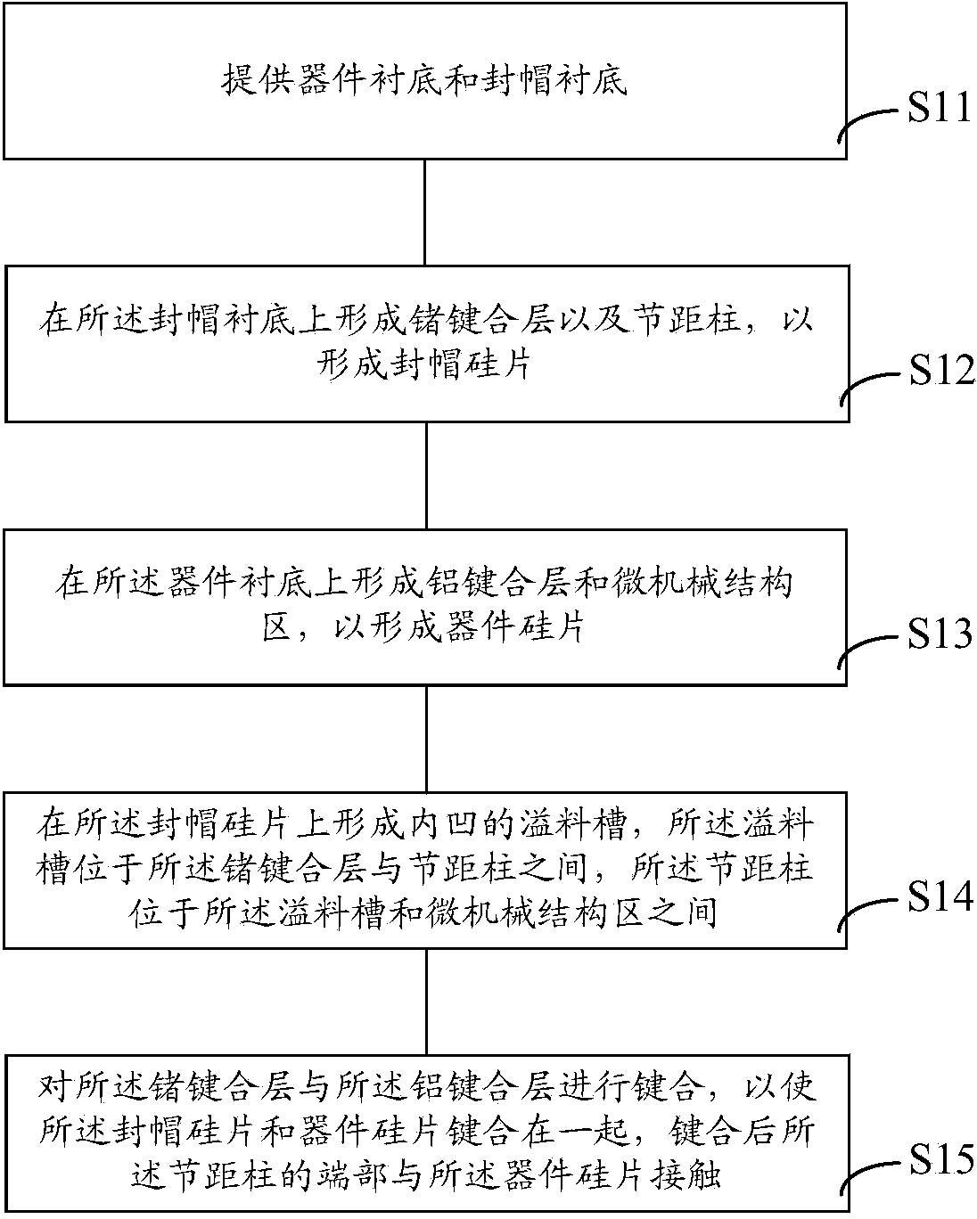
[0048] The present invention will be further described below in conjunction with specific embodiments and accompanying drawings, but the protection scope of the present invention should not be limited thereby.

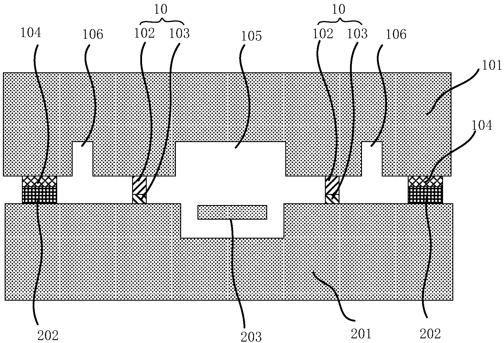
[0049] refer to figure 1 , the MEMS AlGe bonding structure of this embodiment includes a device silicon wafer 201 and a capping silicon wafer 101 that are bonded together. It should be noted that “silicon wafer” is just a commonly used expression in the field, and its material is not limited to silicon, and may also be other substrate materials commonly used in the field of semiconductor technology.

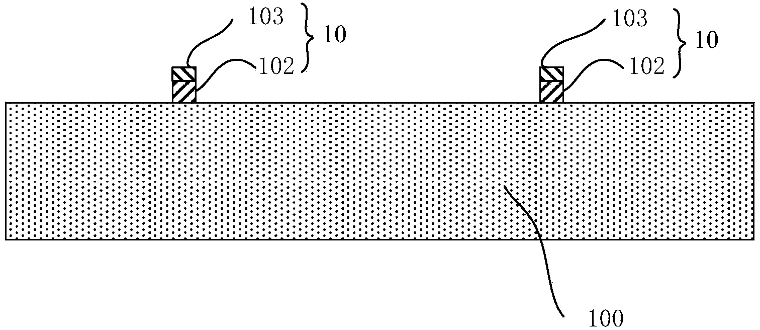
[0050] Among them, a germanium bonding layer 104, a pitch column 10, an overflow groove 106, and a micromechanical structure protection cavity 105 are formed on the capping silicon wafer 101; an aluminum bonding layer 202 and a micromechanical structure area are formed on the device silicon wafer 201. 203. Wherein, the aluminum bonding layer 202 on the device silicon wa...


PUM

PropertyMeasurementUnit
depthaaaaaaaaaa
widthaaaaaaaaaa
widthaaaaaaaaaa

Abstract

The invention provides an MEMS aluminum and germanium bonding structure and a manufacturing method thereof. The structure comprises a device silicon chip and a sealing cap silicon chip, wherein the device silicon chip is provided with a micro mechanical structure area and an aluminum bonding layer; the sealing cap silicon chip is provided with a germanium bonding layer, and the germanium bonding layer is in bonding with the aluminum bonding layer. The sealing cap silicon chip is further provided with a pitch column extending out of the sealing cap silicon chip, and the end of the pitch column is in contact with the device silicon chip. The MEMS aluminum and germanium bonding structure can control aluminum and germanium horizontal extension quantity caused by bonding pressure in the bonding process, and an aluminum and germanium bonding layer with a preset thickness is obtained.

Description

technical field [0001] The invention relates to the technical field of MEMS, in particular to a MEMS aluminum-germanium bonding structure and a manufacturing method thereof. Background technique [0002] MEMS technology is known as a revolutionary high-tech in the 21st century. Its development began in the 1960s. MEMS is the abbreviation of Micro Electro Mechanical System in English, that is, a micro-electromechanical system, which is an ingenious combination of microelectronics and micromechanics. Micro-electro-mechanical systems (MEMS) technology will have a revolutionary impact on human life in the future. The basic technology of MEMS mainly includes silicon anisotropic etching technology, / Silicon bonding technology, surface micro-mechanical technology, LIGA technology, etc., have become indispensable core technologies for the development and production of MEMS. [0003] In the silicon-based MEMS processing technology, some products such as accelerometers, gyroscopes,...

Claims


Application Information

Patent Timeline
Patent Type & Authority Applications(China)
IPC IPC(8): B81B7/02B81C3/00
Inventor 闻永祥范伟宏王平刘琛
Owner HANGZHOU SILAN INTEGRATED CIRCUIT
Why Eureka
Try Eureka