Method for manufacturing high-k dielectric layer water-based indium oxide thin film transistors

A technology of thin film transistors and dielectric layers, which is applied in the manufacture of transistors, semiconductor/solid-state devices, circuits, etc., to reduce costs, avoid high-temperature impurity phases, and realize large-area industrial preparation.

Inactive Publication Date: 2014-08-27
QINGDAO UNIV
View PDF5 Cites 20 Cited by
  • Summary
  • Abstract
  • Description
  • Claims
  • Application Information

AI Technical Summary

Problems solved by technology

Through the review of relevant patents and literature, there are few reports on the preparation of TFT channel layers by

Method used


Image

  • Method for manufacturing high-k dielectric layer water-based indium oxide thin film transistors
  • Method for manufacturing high-k dielectric layer water-based indium oxide thin film transistors
  • Method for manufacturing high-k dielectric layer water-based indium oxide thin film transistors

Examples


Embodiment

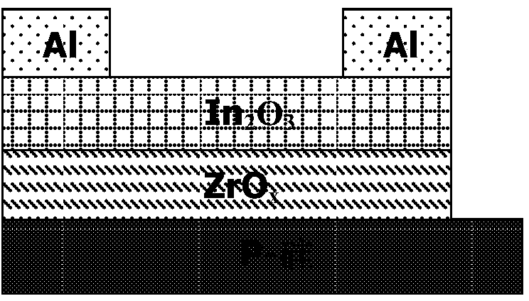
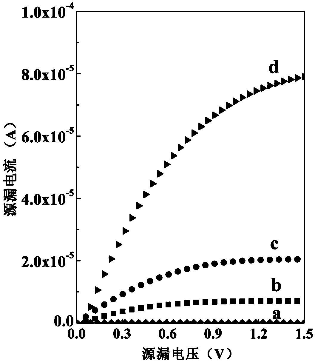
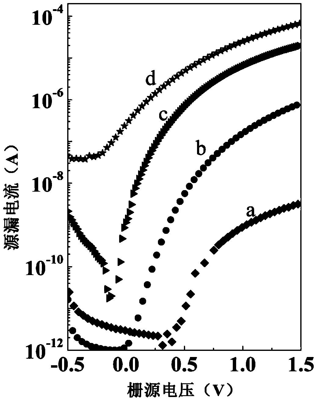
[0019] Zirconium acetylacetonate and indium nitrate powder, dimethylformamide, and ethanolamine organic solvent in this example were all purchased from Aladdin Company, and the purity was greater than 98%; the bottom gate structure was made of ultra-thin zirconia (ZrO x ) is a high-k dielectric layer and water-based indium oxide (In 2 o 3 ) thin film is the preparation process of the thin film transistor of channel layer:

[0020] (1) Ultrathin ZrO was first prepared by sol-gel technique x High-k dielectric films:

[0021] Step 1: Select commercially purchased single-sided polished low-resistance silicon as the substrate (ρ<0.0015Ω·cm) and the gate electrode, and the low-resistance silicon substrate is ultrasonically cleaned with hydrofluoric acid, acetone, and alcohol for 10 minutes each. After repeated washing with deionized water, blow dry with high-purity nitrogen;

[0022] Step 2: Prepare a mixed solution of dimethylformamide and ethanolamine at a molar ratio of 2:1, ...


PUM

PropertyMeasurementUnit
Thicknessaaaaaaaaaa
Thicknessaaaaaaaaaa
Thicknessaaaaaaaaaa

Abstract

The invention belongs to the technical field of manufacturing of semiconductor thin film transistors and relates to a method for manufacturing high-k dielectric layer water-based indium oxide thin film transistors. The method includes the steps that zirconium acetylacetonate is dissolved in dimethylformamide, and ethanol amine of the same molar weight as the zirconium acetylacetonate is added as a stabilizer, so that a precursor solution is formed; a sample is obtained by coating a cleaned low-resistance silicon substrate with the precursor solution in a spinning mode, and a sample obtained after light annealing is obtained by placing the sample below a high-pressure mercury lamp for ultraviolet light treatment; a thin film sample is obtained through annealing of the sample obtained after light annealing; an In2O3 channel layer is obtained by coating the surface of the obtained thin film sample with an In2O3 aqueous solution; finally, a source electrode and a drain electrode are manufactured on the In2O3 channel layer, and then the thin film transistors can be obtained. According to the overall implementation scheme, cost is low, processes are simple, the principle is reliable, product performance is good, the manufacturing process is environmentally friendly, application prospects are wide, and a feasible plan is provided for manufacturing the high-performance thin film transistors on a large scale.

Description

Technical field: [0001] The invention belongs to the technical field of semiconductor thin film transistor preparation, and relates to a method for preparing a high-k dielectric layer water-based indium oxide thin film transistor, in particular to a water-based indium oxide (In 2 o 3 ) as the channel layer and ultra-thin zirconia (ZrO x , 1<x<2) is a method for preparing a thin film transistor with a high-k dielectric layer. Background technique: [0002] In recent years, thin film transistors (Thin Film Transistor, TFT) have played an important role in active matrix liquid crystal display devices (Active Matrix Liquid Crystal Display, AMLCD). From low-temperature amorphous silicon TFT to high-temperature polysilicon TFT, the technology is becoming more and more mature, and the application object has also developed from only driving LCD (Liquid Crystal Display) to driving both LCD and OLED (Organic Light Emitting Display), and even electronic paper . With the conti...

Claims


Application Information

Patent Timeline
IPC IPC(8): H01L29/786H01L29/51H01L21/336
CPCB82Y30/00B82Y40/00H01L21/02282H01L21/02301H01L21/02315H01L21/02348H01L21/02628H01L21/02661H01L21/477H01L29/24H01L29/517H01L29/66969
Inventor 单福凯刘奥刘国侠孟优谭惠月
Owner QINGDAO UNIV
Why Eureka
Try Eureka