Near-infrared sensing chip, preparation method and application thereof
A sensor chip and near-infrared light technology, applied in the field of photoelectric sensors, can solve the problems of unfavorable popularization and development of near-infrared light sensors, inability to face the society and the public, and not easy to operate, so as to reduce the size and cost, and achieve a simple structure. , the effect of convenient operation
- Summary
- Abstract
- Description
- Claims
- Application Information
AI Technical Summary
Problems solved by technology
Method used
Image
Examples
preparation example Construction
[0040] The preparation method of polypyrrole nanoparticles in the following examples: preparation 10mL mass fraction is 0.5% polyvinyl alcohol (molecular weight is 22000) aqueous solution as water phase, 0.4mL pyrrole and 2mL methylene chloride are mixed as oil phase, the two mixed Afterwards, disperse at a speed of 10,000 rpm for 3 minutes under a high-speed disperser, and then add 0.4 mL of saturated ferric chloride solution and stir at a speed of 300 rpm for 12 hours.
[0041] After-treatment to remove the surfactant polyvinyl alcohol (molecular weight: 22000) in the solution, specific steps: add 10 mL of deionized water to the above solution, centrifuge for 20 min at a speed of 10000 rpm in a high-speed centrifuge, and then remove the upper Clear liquid, then add 10mL deionized water to shake, centrifuge, this process is repeated 3 times. The obtained solution is lyophilized in a lyophilizer to obtain polypyrrole nanoparticles for future use.
[0042] The scanning electro...
Embodiment 1
[0044] Embodiment 1, preparation of near-infrared sensor chip and response to near-infrared light
[0045] (1) Preparation of near-infrared sensor chip
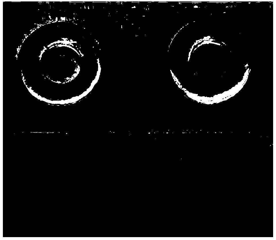
[0046] Precursor and cross-linking agent (model: Sylgard184, two-component reagent, respectively precursor and cross-linking agent; manufacturer: Dow Corning Corporation of the United States) are prepared by a mold to form a PDMS substrate with a mass ratio of 10:1 and a thickness of 2 mm. Then use punches of different diameters, respectively 15mm and 7.5mm, to punch holes in the PDMS substrate based on the same center of circle, to obtain a PDMS annular substrate with through holes, as shown in figure 1 Shown in the middle left figure.
[0047] The upper and lower surfaces of the PDMS ring substrate and the two coverslips were subjected to Plasma treatment (PR-4 glue remover, power: 330W, gas used: air) for two minutes, and then the PDMS substrate and the coverslip were bonded. The bonding process requires heating at 65°C fo...
PUM
 Abstract
Description
Claims
Application Information


