High-density and high-uniform ingan quantum dot structure and growth method

A growth method and quantum dot technology, which is applied in the direction of electrical components, circuits, semiconductor devices, etc., can solve the problem of obtaining high-density, high-uniformity and high-quality InGaN quantum dot materials, restricting the development and application of InGaN quantum dot devices, Problems such as quantum dot damage in processing technology, to achieve the effect of improving device performance, good uniformity, and uniformity without damage

Active Publication Date: 2017-01-25
INST OF SEMICONDUCTORS - CHINESE ACAD OF SCI
View PDF7 Cites 0 Cited by
  • Summary
  • Abstract
  • Description
  • Claims
  • Application Information

AI Technical Summary

Problems solved by technology

The disadvantage is that the parameters such as the position distribution, size and density of quantum dots are discrete and difficult to control, resulting in a wide luminescence spectrum of the material, making it difficult to obtain practical
Although the latter can obtain quantum dots with uniform size and high density, the complex processing technology will bring inevitable additional damage to the quantum dots.
[0004] In summary, the current quantum dot preparation methods are difficult to obtain high-density, high-uniformity and high-quality InGaN quantum dot materials, which seriously restricts the development and application of InGaN quantum dot devices

Method used


Image

  • High-density and high-uniform ingan quantum dot structure and growth method
  • High-density and high-uniform ingan quantum dot structure and growth method

Examples


Embodiment Construction

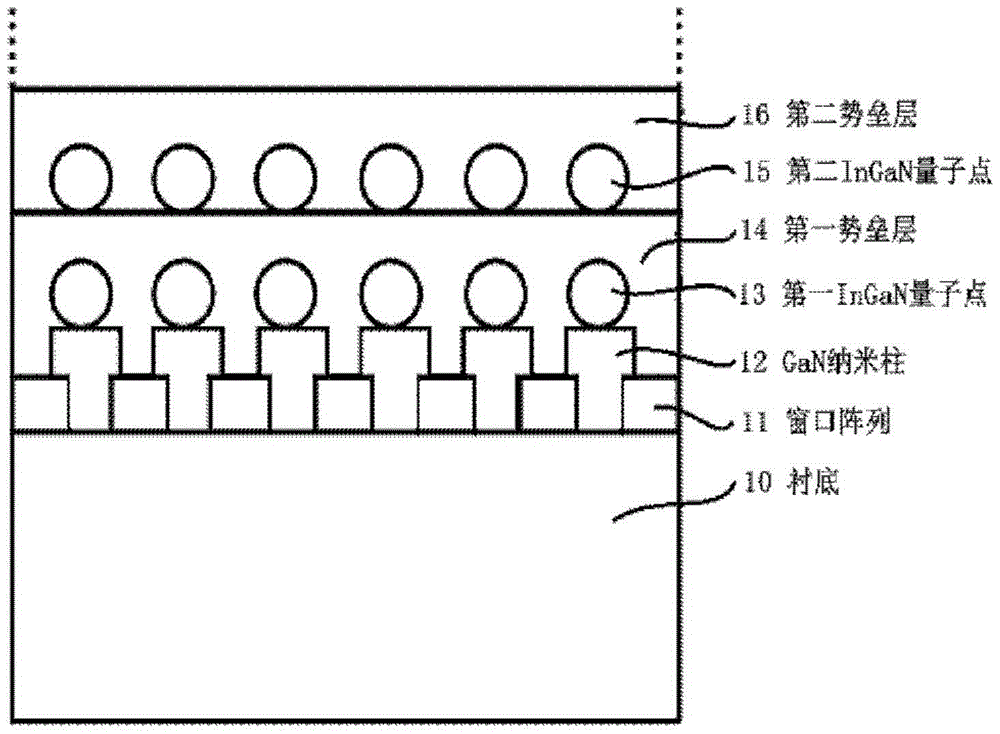
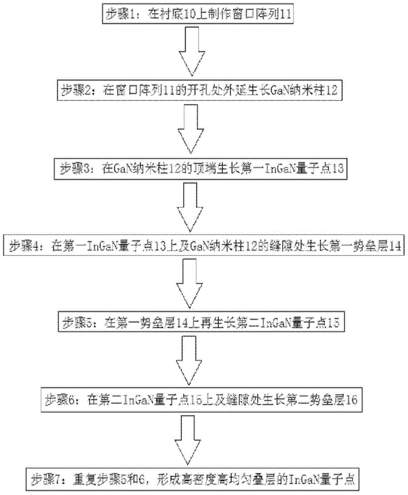
[0030] see figure 1 As shown, the present invention provides a high-density and highly uniform InGaN quantum dot structure, comprising:

[0031] A substrate 10, the material of which can be sapphire, silicon, silicon carbide, gallium nitride or gallium arsenide;

[0032] A window array 11, which is made on the substrate 10, wherein the material of the window array 11 is SiN x or SiO 2 , the aperture of the window array 11 is less than 100nm, and the thickness is about 0.1-5μm. The pattern of the window array 11 is made by electron beam exposure or nanoimprinting technology, so it is possible to obtain tiny windows with extremely high resolution nanoscale dimensions. By adjusting The size and density of the window can change the size and position distribution of quantum dots to realize the regulation of the physical properties of the entire material;

[0033] A GaN nanocolumn 12, which grows at the opening of the window array 11 and is in contact with the surface of the subs...


PUM


Abstract

The invention provides a high density and high uniformity InGaN quantum dot structure and a growth method thereof. The high density and high uniformity InGaN quantum dot structure comprises a substrate, a window array fabricated on the substrate, a GaN nano column array grown at the hole of the window array and is in contact with the surface of the substrate, a first InGaN quantum dot grown at the top of the GaN nano column, a first potential barrier layer which covers the top of the first InGaN quantum dot, a second InGaN quantum dot grown on the first potential barrier layer, a second potential barrier layer which is grown on the first potential barrier layer and coats the second InGaN quantum dot, and a plurality of InGaN quantum dots and potential barrier layers which are orderly grown on the second potential barrier layer repeatedly. The high density and high uniformity InGaN quantum dot structure and the growth method have the double advantages of no defect and high quality of high density and high uniformity and self self-assembly growth of selective growth.

Description

technical field [0001] The invention belongs to the technical field of semiconductors, and in particular relates to a high-density and high-uniform InGaN quantum dot structure and a growth method. It can be used in the fabrication of active regions of semiconductor optoelectronic devices. Background technique [0002] In the past ten years, the preparation technology of GaN series semiconductor materials, especially InGaN materials, has made great progress, which has promoted the rapid development of optoelectronic devices such as semiconductor light-emitting diodes (LEDs) and laser diodes (LDs) in the visible light band. Traditional GaN-based light-emitting devices use InGaN / GaN multiple quantum well structures grown on polar planes. Although the quality of the material grown on the polar plane is high, the quantum confinement Stark effect (QCSE) greatly reduces the luminous efficiency of electron-hole radiation in the quantum well structure, which seriously restricts the ...

Claims


Application Information

Patent Timeline
Patent Type & Authority Patents(China)
IPC IPC(8): H01L33/04H01L33/06H01L33/00
CPCH01L33/0075H01L33/04H01L33/06
Inventor 刘炜赵德刚陈平刘宗顺江德生
Owner INST OF SEMICONDUCTORS - CHINESE ACAD OF SCI
Why Eureka
Try Eureka