
Methods for reducing electrical losses at the gaas/inp interface of bonded multijunction solar cells

A solar cell and bonding technology, applied in circuits, photovoltaic power generation, electrical components, etc., can solve problems that do not involve the electrical properties of the interface, and achieve the effect of low diffusion coefficient

Active Publication Date: 2018-04-17
SHANGHAI INST OF SPACE POWER SOURCES
View PDF8 Cites 0 Cited by
  • Summary
  • Abstract
  • Description
  • Claims
  • Application Information

AI Technical Summary

Problems solved by technology

The bonding method in ref. 2 also does not involve the interface electrical properties reported

Method used

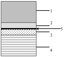

Image

  • Methods for reducing electrical losses at the gaas/inp interface of bonded multijunction solar cells
  • Methods for reducing electrical losses at the gaas/inp interface of bonded multijunction solar cells
  • Methods for reducing electrical losses at the gaas/inp interface of bonded multijunction solar cells

Examples


Embodiment 1

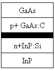
[0053] 1) Bonding layer design and MOCVD epitaxial growth

[0054] The (001) crystal plane n-type InP substrate and p-type GaAs substrate are used, and the doping concentration is 2×10 18 cm -3 , the thickness is 325um. C is used as the p-type dopant. The heavily doped p+GaAs bonding contact layer has a thickness of 40nm and a concentration of 2×10 19 cm -3 . Si is used as the n-type dopant. The thickness of the heavily doped n+InP bonding contact layer is 30nm, and the doping concentration is 7×10 18 cm -3 .

[0055] The bonding contact layer is grown on the GaAs and InP substrates by metal-organic chemical vapor deposition (MOCVD) epitaxial growth method. Using trimethylgallium and trimethylindium as gallium source and indium source respectively, using AsH 3 and PH 3 as a source of arsenic and phosphorus, respectively. The doping source of C is carbon tetrachloride, and the doping source of Si is silane.

[0056] After epitaxial growth such as MOCVD epitaxial gr...

Embodiment 2~5

[0068] Except having changed the bonding temperature in a bonding process to 500, 450, 400, and 350 degreeC respectively, it carried out similarly to Example 1, and obtained samples A2-A5.

Embodiment 6~9

[0070] Except having changed the bonding pressure in the bonding process to 0.5, 2, 12, and 20 MPa, respectively, it carried out similarly to Example 1, and obtained samples A6-A9.


PUM

PropertyMeasurementUnit
thicknessaaaaaaaaaa
surface roughnessaaaaaaaaaa

Abstract

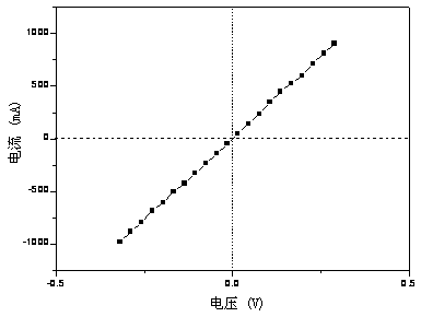
The invention provides a method for reducing bonding multi-junction solar cell GaAs / InP interface electrical loss. The method comprises the following steps: step 1: a GaAs layer acting as a bonding contact layer is prepared on a GaAs substrate via epitaxial growth, and an InP layer acting as another bonding contact layer is prepared on an InP substrate, wherein C is adopted to act as the doping element of the GaAs layer; step 2, surface cleaning and oxide removing are respectively performed on the surface of the GaAs and InP wafers obtained via the step 1 so that the surface of the GaAs and InP wafers after processing is enabled to be a flat surface of which roughness is less than 0.5nm; step 3, the GaAs and InP wafers are laminated and bonded under the conditions of bonding temperature of 400-450 DEG C and pressure of 2-12Mpa, and pre-bonding pressure of 350-450N is applied to the laminated wafers before bonding temperature is reached; and step 4, annealing processing is performed on the wafer set under vacuum atmosphere. A great result of resistivity of 0.26ohm.cm2 of a GaAs / InP bonding interface can be obtained via the method.

Description

technical field [0001] The invention relates to a method for reducing the electrical loss at the GaAs / InP interface of a bonded multi-junction solar cell. Background technique [0002] The traditional triple-junction GaInP / InGaAs / Ge solar cell is a lattice-matched system, and its sub-cell bandgap distribution does not match the solar spectrum. At present, its conversion efficiency is close to the theoretical limit. In order to further improve the conversion efficiency of GaAs multi-junction tandem solar cells, it is necessary to adopt a material system that better matches the solar spectrum. The four-junction cell composed of four sub-cells with band gaps of 1.9eV (GaInP), 1.4eV (GaAs), 1eV (InGaAsP) and 0.7eV (InGaAs) has a band gap distribution that perfectly matches the solar spectrum, and its theoretical efficiency can be significantly promote. However, there is a lattice mismatch of up to 3.8% between InGaAsP / InGaAs sub-cells and GalnP / GaAs cells. The strain generate...

Claims


Application Information

Patent Timeline
Patent Type & Authority Patents(China)
IPC IPC(8): H01L31/18
CPCH01L31/184Y02E10/544Y02P70/50
Inventor 孙利杰陈开建张玮
Owner SHANGHAI INST OF SPACE POWER SOURCES
Learn More