Superconductive nanowire single photon detector with responsivity enhanced based on metamaterials

A single-photon detector and superconducting nanowire technology, applied in the field of detectors, can solve the problems of low absorption efficiency, insufficient response rate, small detection area, etc., so as to reduce the number and probability of photons, improve the absorption efficiency, and improve the absorption rate and response rate

Inactive Publication Date: 2014-12-03
SHANGHAI INST OF TECHNICAL PHYSICS - CHINESE ACAD OF SCI
View PDF3 Cites 13 Cited by
  • Summary
  • Abstract
  • Description
  • Claims
  • Application Information

AI Technical Summary

Problems solved by technology

[0007] The present invention mainly aims at the bottlenecks faced by superconducting nanowire single-photon detectors, such as small detection area, unusable nanowire spacing area, low absorption efficiency, and insufficient response rate, and provides a special material to transfer photons reaching the photosensitive surface A new type of superconducting nanowire single-photon detector that converges to the nanowire region and solves the problem that the light signal in the non-nanowire region cannot be used, thereby enhancing the light absorption efficiency and responsivity

Method used


Image

  • Superconductive nanowire single photon detector with responsivity enhanced based on metamaterials
  • Superconductive nanowire single photon detector with responsivity enhanced based on metamaterials
  • Superconductive nanowire single photon detector with responsivity enhanced based on metamaterials

Examples


Embodiment 1

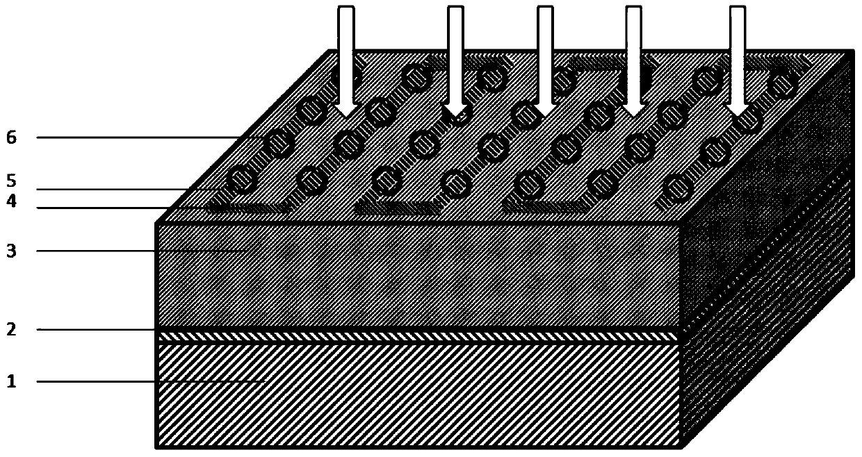
[0040] See figure 1 , a superconducting nanowire single photon detector using an asymmetric metal resonant ring to achieve high light absorption rate and high responsivity, including a substrate 1, a superconducting nanowire 4, a dielectric isolation layer 5 and an asymmetric metal resonant ring array 6 .

[0041] NbN nanowires 4, MgO dielectric spacers 5 and asymmetric metal resonant rings 6 are grown on the MgO substrate 1 sequentially from bottom to top; NbN nanowires have a thickness of 5nm and a width of 120nm, and the distance between adjacent nanowires is 600nm, the duty ratio is 0.2; in order to isolate the superconducting NbN nanowire and the asymmetric metal resonant ring, a MgO isolation layer with a thickness of 5nm is grown on the NbN; finally, the non-opposing metal resonant ring array is processed, and the outer diameter of the unit structure is 170nm, The inner diameter is 120nm, the thickness is 100nm, the material is gold, the corresponding angles of the uno...

Embodiment 2

[0049] See figure 1 , the high light absorption rate, high responsivity superconducting nanowire single photon detector structure of this embodiment.

[0050] The photon coupling resonator includes a metal reflection layer 2, a MgO dielectric layer 3, a NbN nanowire 4, an MgO dielectric isolation layer 5 and an asymmetric metal resonator ring 6 to form a metal-medium-metal (MIM) coupling convergence resonant structure.

[0051] The metal reflection layer 2, the transparent MgO dielectric layer 3, the NbN nanowire 4, the MgO dielectric spacer 5 and the asymmetric metal resonant ring 6 are grown on the MgO substrate 1 sequentially from bottom to top; the material of the metal reflection layer 2 is gold , the thickness is 100nm; the transparent MgO dielectric layer 3 has a thickness of 500nm; NbN nanowires are made on the MgO dielectric layer with a thickness of 5nm and a width of 120nm, the interval between adjacent nanowires is 600nm, and the duty ratio is 0.2; in order to isol...

Embodiment 3

[0061] See figure 1 , the high light absorption rate, high responsivity superconducting nanowire single photon detector structure of this embodiment.

[0062] The photon coupling resonator includes a metal reflection layer 2, a MgO dielectric layer 3, a NbN nanowire 4, an MgO dielectric isolation layer 5 and an asymmetric metal resonator ring 6 to form a metal-medium-metal (MIM) coupling convergence resonant structure.

[0063] The metal reflection layer 2, the transparent MgO dielectric layer 3, the NbN nanowire 4, the MgO dielectric spacer 5 and the asymmetric metal resonant ring 6 are grown on the MgO substrate 1 sequentially from bottom to top; the material of the metal reflection layer 2 is gold , the thickness is 100nm; the transparent MgO dielectric layer 3 has a thickness of 300nm; NbN nanowires are made on the MgO dielectric layer with a thickness of 5nm and a width of 120nm, the interval between adjacent nanowires is 600nm, and the duty ratio is 0.2; in order to isol...


PUM


Abstract

The invention discloses a superconductive nanowire single photon detector with the responsivity enhanced based on metamaterials. The superconductive nanowire single photon detector with the responsivity enhanced based on the metamaterials comprises a substrate, a metal reflecting layer, a dielectric isolation layer, a superconductive nanowire, a dielectric isolation bar and an asymmetric metal ring resonator array, wherein the metal reflecting layer, the dielectric isolation layer, the superconductive nanowire, the dielectric isolation bar and the asymmetric metal ring resonator array are grown on the substrate in sequence from bottom to top, and the superconductive nanowire is separated from the asymmetric metal ring resonator array through the transparent dielectric isolation bar. According to the superconductive nanowire single photon detector with the responsivity enhanced based on the metamaterials, a periodical metamaterial structure is integrated with the superconductive nanowire with the extremely small area, in this way, the number of photons reaching the isolated ineffective area of the superconductive nanowire is greatly reduced, and the probability that the photons reach the isolated ineffective area of the superconductive nanowire is greatly lowered, and both the absorptivity and the responsivity of the superconductive nanowire single photon detector are improved remarkably.

Description

technical field [0001] The invention relates to detector technology, in particular to a superconducting nanowire single-photon detector with high light absorption rate and high responsivity based on enhanced responsivity of metamaterials and a preparation method thereof. Background technique [0002] With the development of detection technology, people's requirements for signal detection sensitivity are gradually increasing. The use of new materials and the advancement of detection methods can detect weak signals covered by noise. In the field of weak signal detection, single photon detection technology is widely used in high-resolution spectral measurement, non-destructive material analysis, high-speed phenomenon detection, precision analysis, atmospheric pollution measurement, bioluminescence, radiation detection, high-energy physics, astronomical photometry, light Time Domain Reflectometry (OTDR), Quantum Key Distribution (QKD) and other fields have a wide range of applic...

Claims


Application Information

Patent Timeline
Patent Type & Authority Applications(China)
IPC IPC(8): H01L39/02H01L39/24
Inventor 陆卫李冠海王少伟陈效双
Owner SHANGHAI INST OF TECHNICAL PHYSICS - CHINESE ACAD OF SCI
Why Eureka
Try Eureka