Inorganic metal oxide semiconductor film of perovskite structure and metallic oxide thin film transistor

A technology of oxide semiconductor and perovskite structure, which is applied in the direction of transistors, semiconductor devices, electrical components, etc., can solve the problems that the back channel etching structure cannot be used, the metal source and drain electrodes cannot be etched, and the production cost is reduced. , to achieve the effect of high current switch ratio, strong acid resistance, and low sub-threshold swing

Active Publication Date: 2014-12-17
SOUTH CHINA UNIV OF TECH
View PDF2 Cites 15 Cited by
  • Summary
  • Abstract
  • Description
  • Claims
  • Application Information

AI Technical Summary

Problems solved by technology

[0005]At present, indium gallium zinc oxide (IGZO) is a representative of MO semiconductor materials, but its band gap is between 2.8 and 3.2eV, and it is suitable for ultraviolet or ultraviolet light There is still a large absorption, resulting in instability under light
In addition, IGZO contains a large amount of indium, and usually large-scale new flat panel display indium content In/(In+Zn+Ga)>0.33, resulting in higher cost
In addition, most of the current MO semiconductor materials are sensitive

Method used


Image

  • Inorganic metal oxide semiconductor film of perovskite structure and metallic oxide thin film transistor
  • Inorganic metal oxide semiconductor film of perovskite structure and metallic oxide thin film transistor
  • Inorganic metal oxide semiconductor film of perovskite structure and metallic oxide thin film transistor

Examples


Embodiment 1

[0041]A metal oxide thin film transistor is provided with a gate, an active layer, an insulating layer between the gate and the active layer, a source and a drain electrically connected to both ends of the active layer, and a passivation layer, The active layer is an inorganic metal oxide semiconductor film with a perovskite structure, and the active layer covers the insulating layer.

[0042] It should be noted that the upper and lower positional relationship in the present invention is a reference positional relationship with the substrate as the lower layer.

[0043] It should be noted that the metal oxide thin film transistor of the present invention may be a structure including only a substrate, a gate, an insulating layer, an active layer, a source electrode and a drain electrode, and a passivation layer, and may further include an etch stop layer Or pixel definition layer, etc., and can also be integrated with other devices and other structures.

[0044] Specifically, ...

Embodiment 2

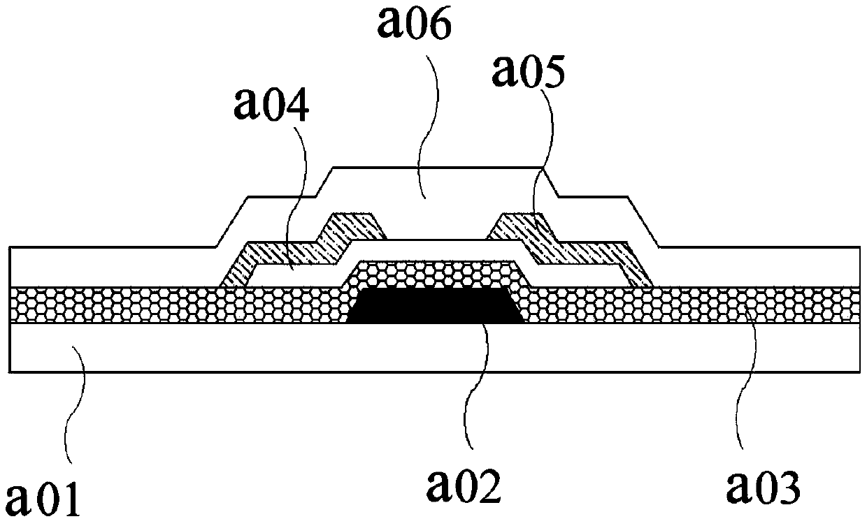
[0055] A metal oxide thin film transistor, such as figure 1 As shown, the thin film transistor has a back channel etching structure, and is provided with a substrate a01, a gate a02, an insulating layer a03, an active layer a014, a source-drain electrode a05, and a passivation layer a06.

[0056] The gate a02 is located on the substrate a01, the insulating layer a02 is located on the substrate and the gate, the active layer a02 covers the upper surface of the insulating layer and corresponds to the gate, the source and the drain are spaced from each other and connected to the active layer respectively. The electrodes at both ends of the source layer are connected, and the passivation layer a06 covers the upper surface of the exposed surfaces of the active layer, the source electrode and the drain electrode.

[0057] The substrate a01 may be a glass substrate, a metal substrate, or a polymer substrate. The substrate has a buffer layer and a water and oxygen barrier layer. Whe...

Embodiment 3

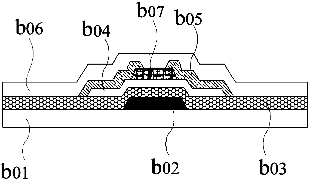
[0077] A metal oxide thin film transistor, such as figure 2 As shown, the thin film transistor has an etch stop structure, and is provided with a substrate b071, a gate b02, an insulating layer b03, an active layer b04, a source-drain electrode b05, and a passivation layer b06, and the active layer covers the insulating layer. The thin film transistor is also provided with an etch stop layer b07. The etch stop layer b07 is SiO x 、SiN x o y 、SiN x , SiC, Al 2 o 3 or ZrO2 Thin films with a thickness of 100 nm to 200 nm.

[0078] The structures and preparation methods of the substrate b071 , the gate b02 , the insulating layer b03 , the active layer b04 , the source-drain electrodes b05 , and the passivation layer b06 are the same as those in Embodiment 2, and will not be repeated here.

[0079] The metal oxide thin film transistor of the present invention adopts an inorganic metal oxide semiconductor thin film with a nanocrystalline perovskite structure as an active laye...


PUM

PropertyMeasurementUnit
Thicknessaaaaaaaaaa
Thicknessaaaaaaaaaa
Thicknessaaaaaaaaaa

Abstract

The invention provides an inorganic metal oxide semiconductor film of a perovskite structure and a metallic oxide thin film transistor. The inorganic metal oxide semiconductor film of the perovskite structure is used as an active layer. The inorganic metal oxide semiconductor film of the perovskite structure is expressed as the chemical expression: MxA1-xBo3, wherein 0.01<=x<=0.5, A is at least one chemical element of Ca, Sr and Ba, B is a chemical element of Ti and Sn, and M is at least one chemical element of Sc, Y, rare earth elements, Al and In. The inorganic metal oxide semiconductor film of the perovskite structure is composed of crystal particles of the perovskite structure, and sizes of the crystal particles vary from 2mm to 900mm. The thickness of the inorganic metal oxide semiconductor film of the perovskite structure varies from 10nm to 500nm. When the inorganic metal oxide semiconductor film of the perovskite structure is used as the active layer, electronic mobility is high, and the metallic oxide thin film transistor prepared by using the inorganic metal oxide semiconductor film of the perovskite structure is good in light stability, low in sub-threshold swing amplitude, simple in preparation technology and low in cost.

Description

technical field [0001] The invention relates to the technical field of semiconductors, in particular to an inorganic metal oxide semiconductor thin film with a perovskite structure as an active layer and a metal oxide thin film transistor having the thin film. Background technique [0002] Thin Film Transistor (TFT, Thin Film Transistor) is mainly used to control and drive sub-pixels of Liquid Crystal Display (LCD, Liquid Crystal Display) and Organic Light-Emitting Diode (OLED, Organic Light-Emitting Diode) displays, and is the most important in the field of flat panel display. One of the electronic devices. With consumers' high demand for large-size, high-resolution flat-panel displays, thin-film transistor (TFT) backplane technology is also undergoing profound changes. [0003] The traditional amorphous silicon (a-Si) semiconductor TFT has low mobility (generally less than 0.5cm 2 / (V·s)), it is difficult to achieve high-resolution display, and is facing the fate of bein...

Claims


Application Information

Patent Timeline
IPC IPC(8): H01L29/786H01L29/43
Inventor 兰林锋彭俊彪王磊林振国
Owner SOUTH CHINA UNIV OF TECH
Why Eureka
Try Eureka