N type PERC crystalline silicon solar cell and preparation method thereof
A technology of solar cells and crystalline silicon, applied in circuits, photovoltaic power generation, electrical components, etc., can solve problems such as scarcity of technical solutions, and achieve the effects of improving technical assurance, convenient operation, and good economic benefits
- Summary
- Abstract
- Description
- Claims
- Application Information
AI Technical Summary
Problems solved by technology
Method used
Image

Examples
Embodiment 1
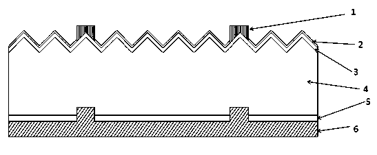
[0041] In this embodiment, a 156mm N-type single crystal silicon wafer is used as the base material to remove damage, texture, and clean the N-type silicon wafer; a P-type emitter junction is formed by using tubular boron diffusion, and the diffusion resistance is controlled at 80 ohm / sq. The borosilicate glass naturally formed by diffusion is used as the front mask of the battery to achieve the purpose of removing the reflective junction and polishing on the back of the silicon wafer. Clean with 1% hydrofluoric acid solution. An aluminum oxide passivation film with a thickness of 15nm is symmetrically grown on the front and back of the silicon wafer, and a silicon nitride anti-reflection film with a refractive index of 2.10 and a thickness of 68nm is grown on the front of the silicon wafer by PECVD. Print silver-aluminum paste grid lines on the front side of the silicon wafer and sinter the metal to metallize the electrodes. On the back side of the silicon wafer, use a line a...
Embodiment 2
[0045] In this embodiment, a 156mm N-type single crystal silicon wafer is used as the base material to remove damage, texture, and clean the N-type silicon wafer; a P-type emitter junction is formed by using tubular boron diffusion, and the diffusion resistance is controlled at 45 ohm / sq. The borosilicate glass naturally formed by diffusion is used as the front mask of the battery to achieve the purpose of removing the reflective junction and polishing on the back of the silicon wafer. Clean with 1% hydrofluoric acid solution. An aluminum oxide passivation film with a thickness of 2nm is symmetrically grown on the front and back of the silicon wafer, and a silicon nitride anti-reflection film with a refractive index of 1.9 and a thickness of 90nm is grown on the front of the silicon wafer by PECVD. The front side of the silicon wafer is printed with silver-aluminum paste grid lines and sintered metal to metallize the electrodes. On the back of the silicon wafer, the aluminum o...
Embodiment 3
[0049]In this embodiment, a 156mm N-type single crystal silicon wafer is used as the base material to remove damage, texture, and clean the N-type silicon wafer; a P-type emitter junction is formed by using tubular boron diffusion, and the diffusion resistance is controlled at 140 ohm / sq. The borosilicate glass naturally formed by diffusion is used as the front mask of the battery to achieve the purpose of removing the reflective junction and polishing on the back of the silicon wafer. Clean with 1% hydrofluoric acid solution. An aluminum oxide passivation film with a thickness of 40nm is symmetrically grown on the front and back of the silicon wafer, and a silicon nitride antireflection film with a refractive index of 2.3 and a thickness of 50nm is grown on the front of the silicon wafer by PECVD. Silver-aluminum paste grid lines are printed on the front side of the silicon wafer and the metal is sintered to metallize the electrodes. On the back side of the silicon wafer, the...
PUM
| Property | Measurement | Unit |
|---|---|---|
| Thickness | aaaaa | aaaaa |
| Thickness | aaaaa | aaaaa |
| Thickness | aaaaa | aaaaa |
Abstract
Description
Claims
Application Information
 - Generate Ideas
- Intellectual Property
- Life Sciences
- Materials
- Tech Scout
- Unparalleled Data Quality
- Higher Quality Content
- 60% Fewer Hallucinations
Browse by: Latest US Patents, China's latest patents, Technical Efficacy Thesaurus, Application Domain, Technology Topic, Popular Technical Reports.
© 2025 PatSnap. All rights reserved.Legal|Privacy policy|Modern Slavery Act Transparency Statement|Sitemap|About US| Contact US: help@patsnap.com