Gallium Nitride-Based Heterojunction Field-Effect Transistor with Internal Composite Field Plate Structure

A heterojunction field effect and body recombination technology, which is applied in semiconductor devices, electrical components, circuits, etc., can solve the problem that N-type channel doping cannot be allowed, the withstand voltage capacity is only equivalent to ordinary, and the breakdown voltage of devices can be reduced. problems, to achieve the effect of reducing the possibility, raising the electric field, and reducing the on-resistance

Active Publication Date: 2018-04-20
UNIV OF ELECTRONICS SCI & TECH OF CHINA
View PDF6 Cites 0 Cited by
  • Summary
  • Abstract
  • Description
  • Claims
  • Application Information

AI Technical Summary

Problems solved by technology

Although this technology has not been realized yet, theoretical analysis shows that the direct contact between the metal electrode and the semiconductor cannot reduce the leakage current. On the contrary, because of its good conductivity, it is easier to form a buffer layer leakage channel, thereby reducing the breakdown voltage of the device.
In addition, the distance between the internal electrode and the drain is relatively close, and there is only a PN junction structure in the middle, and its reverse leakage is very large. If the internal electrode is connected to the source or gate, the withstand voltage capability of the entire device is only equivalent to Compared with ordinary GaN PN junction
In addition to the impact on the breakdown voltage described in the above two points, this structure cannot allow a higher concentration of N-type channel doping to reduce the on-resistance, so it is difficult to improve the figure of merit (FOM) of the device

Method used


Image

  • Gallium Nitride-Based Heterojunction Field-Effect Transistor with Internal Composite Field Plate Structure
  • Gallium Nitride-Based Heterojunction Field-Effect Transistor with Internal Composite Field Plate Structure
  • Gallium Nitride-Based Heterojunction Field-Effect Transistor with Internal Composite Field Plate Structure

Examples


Embodiment

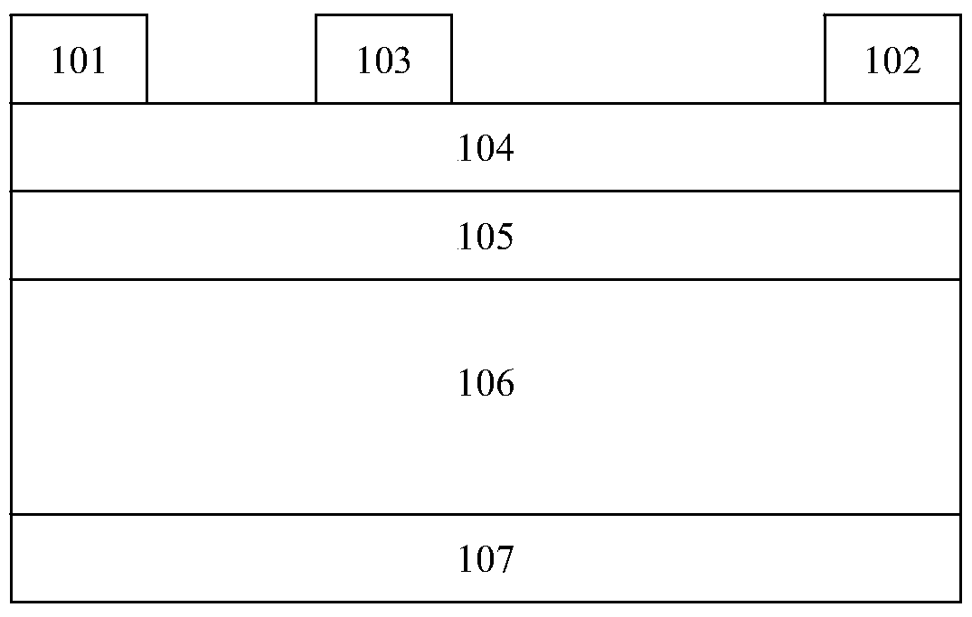
[0025] see figure 1, is a structural schematic diagram of an existing GaN HFET device, including a substrate 107, a gallium nitride (GaN) buffer layer 106, a gallium nitride (GaN) channel layer 105, an aluminum gallium nitride (AlGaN) barrier layer 104 and an aluminum A source 101, a drain 102 and a gate 103 are formed on a gallium nitride (AlGaN) barrier layer 104, wherein the gallium nitride buffer layer 106 is disposed above the substrate 107, and the gallium nitride channel layer 105 is disposed on the gallium nitride Above the buffer layer 106, the AlGaN barrier layer 104 is arranged above the GaN channel layer 105, the source electrode 101 and the drain electrode 102 form an ohmic contact with the AlGaN barrier layer 104, and the gate electrode 103 is in contact with the AlGaN barrier layer 104. Gallium nitride (AlGaN) barrier layer 104 forms a Schottky contact.

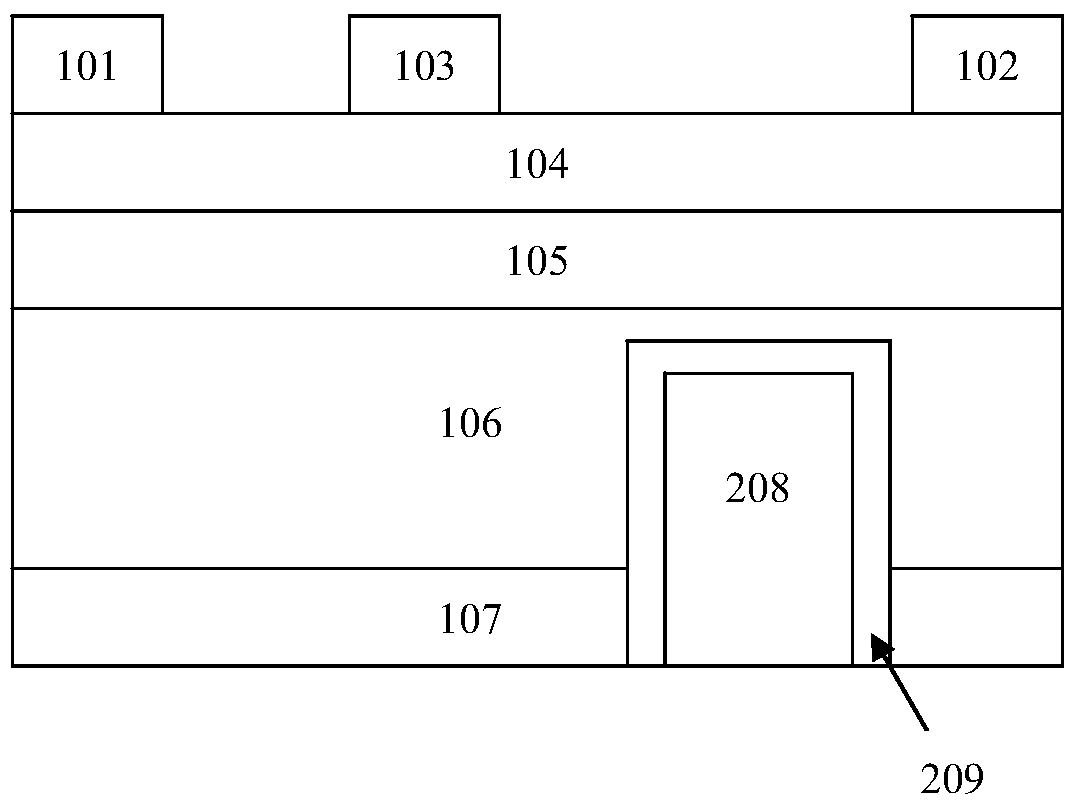
[0026] see figure 2 , is a structural schematic diagram of a gallium nitride-based heterojunction field e...


PUM


Abstract

The present invention relates to semiconductor technology. The invention solves the problem of low withstand voltage of the existing gallium nitride-based heterojunction field effect transistor, and provides a gallium nitride-based heterojunction field effect transistor with an internal compound field plate structure, and its technical scheme can be summarized For: Compared with the existing common GaN HFET (gallium nitride-based heterojunction field effect transistor), the gallium nitride-based heterojunction field effect transistor with internal composite field plate structure of the present invention also has internal composite field plate Structure, the compound field plate structure in the body is composed of electrodes and insulating dielectric layers. The beneficial effect of the invention is that the withstand voltage of the device is increased, and the invention is suitable for GaN-based heterojunction field effect transistors.

Description

technical field [0001] The invention relates to semiconductor technology, in particular to gallium nitride (GaN)-based heterojunction field effect transistor strained N-channel metal oxide semiconductor field effect transistor (NMOSFET). Background technique [0002] Gallium nitride (GaN)-based heterojunction field effect transistor (HFET) has excellent characteristics such as large band gap, high critical breakdown electric field, high electron saturation velocity, good thermal conductivity, radiation resistance and good chemical stability. GaN materials can form two-dimensional electron gas heterojunction channels with high concentration and high mobility with materials such as aluminum gallium nitride (AlGaN), so they are especially suitable for high-voltage, high-power and high-temperature applications, and are the most suitable for power electronics applications. One of the most promising transistors. [0003] figure 1 It is a schematic structural diagram of a common ...

Claims


Application Information

Patent Timeline
Patent Type & Authority Patents(China)
IPC IPC(8): H01L29/778H01L29/06
CPCH01L29/407H01L29/778
Inventor 杜江锋陈南庭潘沛霖刘东于奇
Owner UNIV OF ELECTRONICS SCI & TECH OF CHINA
Why Eureka
Try Eureka