


Quick Research
Generate reliable direction feasibility study reports for your R&D in just a few steps.

Technical Q&A
Discover and master advanced knowledge NOW. Basics, ideas, possibilities, all at once.

Find Solutions
As an expert in R&D theories, this can generate solutions to your technical problems instantly.

Evaluate Feasibility
Analyze your overall solution with one click, know your potential R&D risks in advance.

Monitor Landscape
Get weekly tech updates, stay abreast of the latest tech innovations and key insights.
A method for preparing nanoscale field effect transistors
A field effect transistor, nanoscale technology, applied in nanotechnology, nanotechnology, nanotechnology for information processing, etc., can solve the problems of increasing device fluctuations and parasitic effects, difficult to obtain, etc., to reduce parasitic and The effect of fluctuation, low cost and simple process
- Summary
- Abstract
- Description
- Claims
- Application Information
AI Technical Summary
Problems solved by technology
Method used
Image

Examples
Embodiment Construction
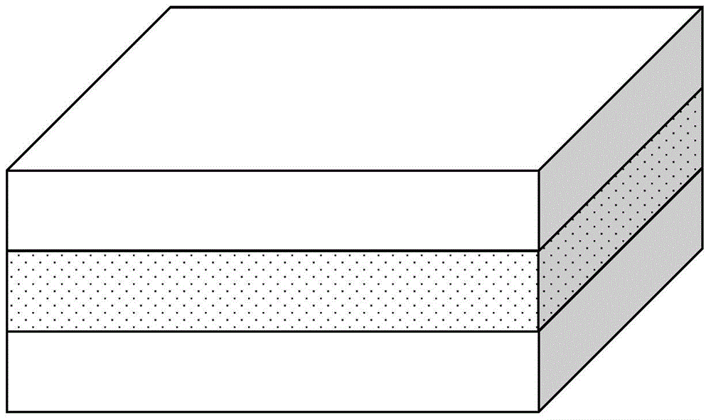
[0038] Taking a silicon substrate as an example, the specific implementation of the method for preparing a nanoscale field effect transistor by epitaxial growth on an SOI substrate of the present invention is as follows:
[0039] 1. Thinned SOI silicon substrate
[0040] a) The thickness of the SOI silicon substrate is Such as figure 1 shown;
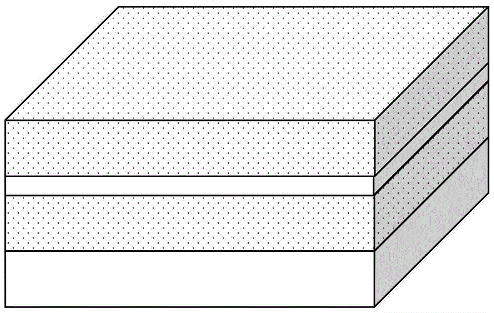
[0041] b) Dry oxygen oxidation forms a sacrificial oxide layer on the SOI silicon substrate Thinning the silicon film to Such as figure 2 shown;
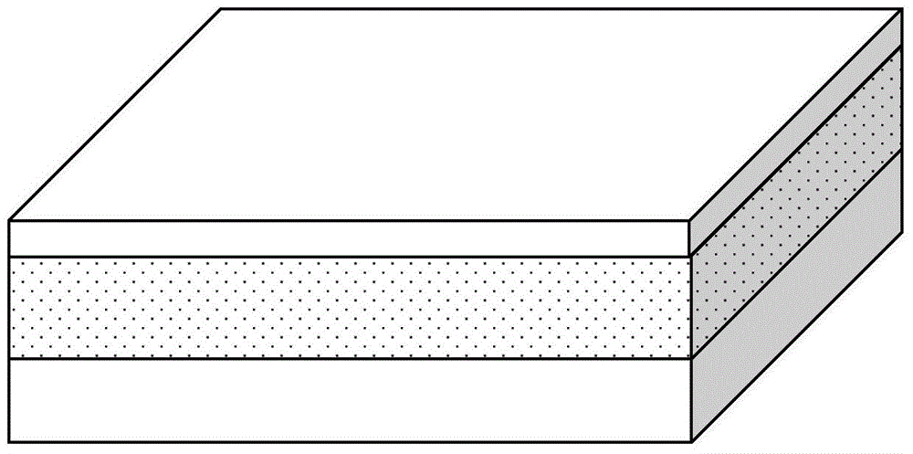
[0042] c) HF solution wet etching to remove the sacrificial oxide layer Such as image 3 shown;
[0043] 2. Source-drain doping;
[0044] a) Ion implantation injecting P, the dose is 1×10 15 cm -2 , doping the SOI silicon substrate;
[0045] b) Rapid thermal annealing (RTP) at 950°C for 5s for impurity activation annealing, such as Figure 4 shown;
[0046] 3. Silicon thin line structure;
[0047] a) Electron beam lithography forms a thin line pattern with a width of 20nm...
PUM
 Abstract
Description
Claims
Application Information
 - R&D Engineer
- R&D Manager
- IP Professional
- Industry Leading Data Capabilities
- Powerful AI technology
- Patent DNA Extraction
Browse by: Latest US Patents, China's latest patents, Technical Efficacy Thesaurus, Application Domain, Technology Topic, Popular Technical Reports.
© 2024 PatSnap. All rights reserved.Legal|Privacy policy|Modern Slavery Act Transparency Statement|Sitemap|About US| Contact US: help@patsnap.com