Preparation method of large-scale array graphene nanoelectronic resonator based on femtosecond laser

A femtosecond laser and nano-electromechanical technology, applied in the process of producing decorative surface effects, manufacturing microstructure devices, decorative arts, etc., can solve the secondary pollution of graphene, reduce the resonance frequency and quality factor of nano-electromechanical resonators and other issues, to achieve the effect of improving resonance frequency and quality factor, reducing secondary pollution, and reducing production costs

Active Publication Date: 2015-01-28
JIANGSU UNIV
View PDF8 Cites 4 Cited by
  • Summary
  • Abstract
  • Description
  • Claims
  • Application Information

AI Technical Summary

Problems solved by technology

It involves etching a large-area graphene film, which requires spin-coating photoresist and plasma etching technology, which will

Method used


Image

  • Preparation method of large-scale array graphene nanoelectronic resonator based on femtosecond laser
  • Preparation method of large-scale array graphene nanoelectronic resonator based on femtosecond laser

Examples


Embodiment Construction

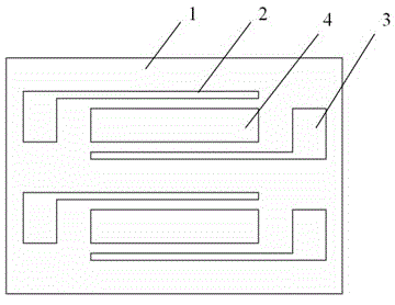
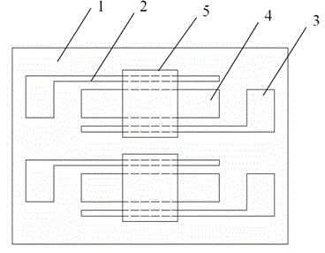
[0017] see figure 1 and figure 2 , the present invention first SiO 2 The surface of / Si substrate 1 is patterned by conventional reactive ion etching (RIE) to form a patterned substrate, and then large-area graphene 5 is transferred to the surface of the patterned substrate, and finally processed by femtosecond laser micromachining technology Etching large-scale arrays of graphene nanoelectromechanical resonators. The specific implementation steps are as follows:

[0018] 1. Thermally grow 300 nm thick SiO on the surface of n-type Si substrate 2 insulating layer, forming SiO 2 / Si substrate 1 . Wherein, the resistivity of the n-type Si substrate is 1~10 Ωcm.

[0019] 2. In SiO 2 The surface of Si substrate 1 is sputtered with 5 nm thick TiW alloy and 100 nm thick Au; photolithography is carried out with No. 1 mask plate, after development, TiW / Au is etched in a metal corrosion solution to form an array of TiW / Au The wiring 2 and the Au electrode sheet 3 of the array. ...


PUM

PropertyMeasurementUnit
Resistivityaaaaaaaaaa

Abstract

The invention discloses a preparation method of a large-scale array graphene nanoelectronic resonator based on femtosecond laser. The preparation method comprises the following steps: sputtering a TiW alloy and Au on the surface of a SiO2/Si substrate; preparing a single-layered graphene thin film by a chemical vapor deposition method; transferring the single-layered graphene thin film onto TiW/Au connection wires; and scanning and cutting the two adjacent TiW/Au connection wires and a single-layered graphene thin film region between two adjacent Au electrode sheets by adopting the femtosecond laser to form the array graphene nanoelectronic resonator, wherein the energy density of the femtosecond laser is more than 0.16J/cm<2>-0.21J/cm<2>. According to the preparation method of the large-scale array graphene nanoelectronic resonator based on the femtosecond laser, a traditional CMOS process is combined with a preparation process of a femtosecond laser micro-machining technology and a preparation technology from bottom to top is completely adopted; photoresist does not need to be spun and plasma etching is avoided; the secondary pollution to graphene is reduced and the resonant frequency and the quality factor of the nanoelectronic resonator are greatly improved; and meanwhile, the manufacturing cost is extremely reduced.

Description

technical field [0001] The invention belongs to the application field of nano-electromechanical systems (NEMS), and relates to a batch array preparation method of graphene nano-electromechanical resonators. Background technique [0002] The nanoelectromechanical resonator is the basic structure and typical device of the nanoelectromechanical system. Through the change of the effective mass of the cantilever beam of the nanoelectromechanical resonator, it can monitor infectious pathogens, toxic chemical gases and explosives in the environment in real time. It can be used to characterize biochemical reactions. [0003] Graphene is the best material for detecting biochemical molecules due to the following characteristics: 1. Graphene is a strictly two-dimensional material with a high specific surface area. Under the same volume, the molecules adsorbed on the surface of graphene are the largest compared with other materials; 2. Graphene has strong electrical conductivity and sh...

Claims


Application Information

Patent Timeline
IPC IPC(8): B81C1/00
Inventor 王权白冰刘帅郑蓓蓉薛伟
Owner JIANGSU UNIV
Why Eureka
Try Eureka