
Method for preparing novel GaN-based laser and GaN-based laser

A laser, a new type of technology, applied in lasers, laser parts, semiconductor lasers, etc., can solve epitaxial wafers that cannot be purchased from abroad for GaN-based lasers, GaN laser chips are difficult to prepare, development constraints, etc. problem, to achieve the effect of improving the light confinement effect, increasing the recombination efficiency, and increasing the confinement factor

Active Publication Date: 2015-01-28
DONGGUAN INST OF OPTO ELECTRONICS PEKING UNIV +1
View PDF7 Cites 12 Cited by
  • Summary
  • Abstract
  • Description
  • Claims
  • Application Information

AI Technical Summary

Problems solved by technology

Laser display has now become a new field for my country to accelerate technological innovation. It has received strong support from the state in the early stage. Gallium nitride-based blue lasers, as the core components of portable laser displays, can create more new display products. The estimated market value is very high. Remarkably, some domestic companies have identified the market and are already conducting technical research and trial production. However, due to the difficulty in the preparation of gallium nitride laser chips, which require a lot of investment in funds and technical strength, the core technology has been used by Japan, Large companies in the United States, Germany and South Korea have mastered it, and it is still impossible to purchase GaN-based laser epitaxial wafers from abroad, and the development of this field in China is greatly restricted.

Method used


Image

  • Method for preparing novel GaN-based laser and GaN-based laser
  • Method for preparing novel GaN-based laser and GaN-based laser

Examples


Embodiment 1

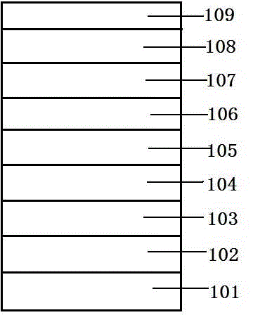
[0032] Use Aixtron company, tightly coupled vertical reaction chamber MOCVD growth system. During the growth process, at least one of trimethylgallium (TMGa), trimethylindium (TMIn), trimethylaluminum (TMAl) was used as a group III source, ammonia gas (NH 3 ) as the Group V source, silane (SiH 4 ) as an n-type dopant source, magnesiumocene (Cp 2 Mg) as a p-type dopant source, firstly heat the GaN substrate 101 to 1050 degrees Celsius in the MOCVD reaction chamber, hydrogen (H 2 ) atmosphere, using TMGa as the III source, NH 3 As a Group V source, SiH 4 4 micron thick n-GaN 102 grown as an n-type dopant source with an electron concentration of 5×10 18 cm -3 ; in hydrogen (H 2 ) atmosphere, at 850 ° C ~ 1050 ° C, using TMGa, TMAl and TMIn as the group III source, NH 3 As a group V source, SiH4 is used as an n-type dopant source to grow 150 cycles of modulation-doped Al composition and n-Al with In composition and asymmetric structure 0.15 Ga 0.85 N / GaN / Al 0.15 In 0....


PUM

PropertyMeasurementUnit
thicknessaaaaaaaaaa
wavelengthaaaaaaaaaa
thicknessaaaaaaaaaa

Abstract

The invention provides a method for preparing a novel GaN-based laser and a GaN-based laser. According to the method of the invention, a series of critical technologies and scientific problems in the preparation of a GaN-based laser can be solved through adopting a metal organic chemical compound vapor phase epitaxy technique. According to the technical scheme of the invention, the method for preparing the novel GaN-based laser includes the step that with trimethylgallium, trimethylindium and trimethylaluminum adopted as a III-family source, ammonia adopted as a V-family source, and silane adopted as an n type doping source, and magnesocene adopted as a P type doping source, the metal organic chemical compound vapor phase epitaxy technique is utilized to prepare the novel GaN-based laser. According to the method for preparing the novel GaN-based laser of the invention, a multi-cycle In component linear graded InxGa1-xN / GaN superlattice structure, replacing a traditional single GaN layer, is adopted as the waveguide layer of the GaN-based blue laser, and therefore, limiting factors of a light field in a laser emission region can be effectively improved, and the gain of the active regions of quantum wells can be improved.

Description

technical field [0001] The invention belongs to the technical field of semiconductor optoelectronics, in particular to a method for preparing a novel GaN-based laser and a GaN-based laser. Background technique [0002] Since the invention of semiconductor laser diodes half a century ago, semiconductor lasers in the infrared and red bands based on gallium arsenide and indium phosphide semiconductors have developed rapidly, and their application range covers the entire field of optoelectronics. various aspects of the field. Green or blue semiconductor lasers with shorter wavelengths than red light are widely used in laser display, underwater communication, laser printing, high-density information reading and writing, and deep water detection. Because the gallium nitride material has a wide energy band, the wavelength of the gallium nitride laser can cover a wide range from infrared to visible light to ultraviolet by adjusting the alloy composition. It is currently the best ch...

Claims


Application Information

Patent Timeline
Patent Type & Authority Applications(China)
IPC IPC(8): H01S5/343H01S5/30
Inventor 贾传宇张国义童玉珍
Owner DONGGUAN INST OF OPTO ELECTRONICS PEKING UNIV
Learn More