Three-dimensional MoS2 / SnO2 heterogeneous semiconductor nano material and preparation method thereof

A nanomaterial and semiconductor technology, applied in the field of three-dimensional MoS2/SnO2 heterogeneous semiconductor nanomaterials and its preparation, can solve the problems of inapplicability to large-scale industrial production, high production costs, harsh reaction conditions, etc.

Inactive Publication Date: 2015-02-04
EAST CHINA NORMAL UNIVERSITY
View PDF2 Cites 14 Cited by
  • Summary
  • Abstract
  • Description
  • Claims
  • Application Information

AI Technical Summary

Problems solved by technology

Recently, MoS 2 /SnO 2 The structural system has attracted the attention of many researchers, and various methods have been used to prepare various MoS 2 /SnO 2

Method used


Image

  • Three-dimensional MoS2 / SnO2 heterogeneous semiconductor nano material and preparation method thereof
  • Three-dimensional MoS2 / SnO2 heterogeneous semiconductor nano material and preparation method thereof
  • Three-dimensional MoS2 / SnO2 heterogeneous semiconductor nano material and preparation method thereof

Examples


Embodiment 1

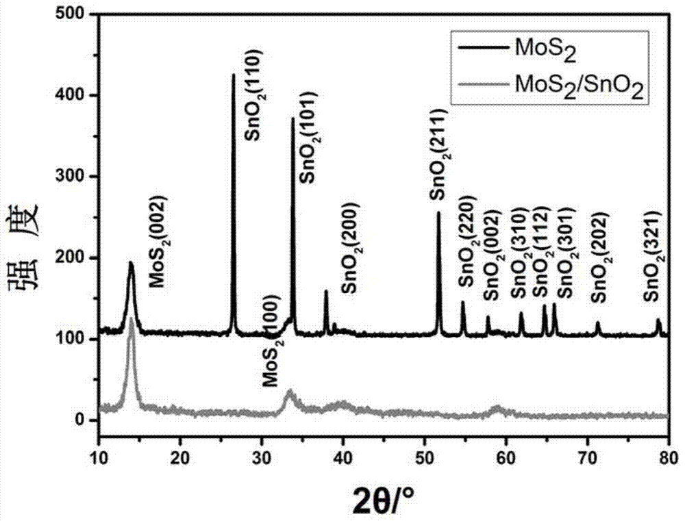
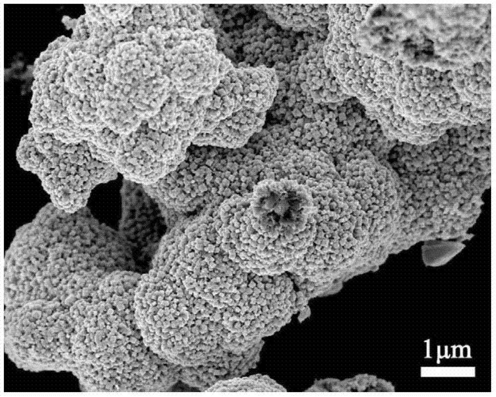
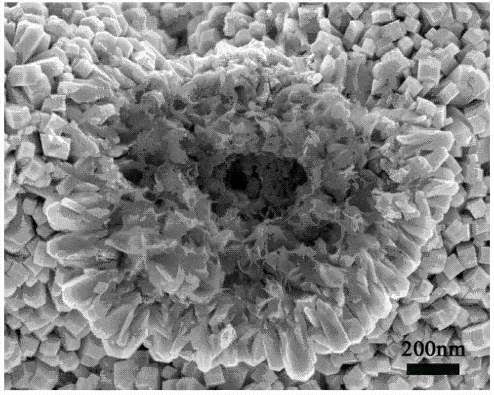
[0031] Example 1 Three-dimensional MoS of the present invention 2 / SnO 2 Fabrication of heterogeneous semiconducting nanostructures

[0032] The concrete steps of preparation method are as follows:

[0033] a. Mix 1.0g of sodium molybdate, 1.2g of thiourea and 0.4g of oxalic acid and dissolve in 80mL of deionized water, and stir thoroughly for 20 minutes.

[0034] b. Then transfer the mixed solution into a 100mL reaction kettle, place the reaction kettle in a vacuum oven and heat it at 200°C for 24 hours. When the reaction is completed and cooled to room temperature, collect the black reaction product and wash it repeatedly with deionized water and absolute ethanol Several times until the supernatant is completely clear.

[0035] c. Pour off the supernatant, dry the pure sample in a vacuum oven at 60° C. for 5 hours, and then take it out to obtain a black powder.

[0036] d. Place the black powder in a vacuum furnace protected by pure argon, burn it at 850°C for 2 hours, a...

Embodiment 2

[0041] Embodiment 2 The three-dimensional M of the present invention o Preparation of S2 / SnO2 Hetero-Semiconductor Nanostructures

[0042] In this example, step a is to mix 1.0g of sodium molybdate, 1.2g of thiourea and 0.25g of oxalic acid, dissolve them in 80mL of deionized water, and stir them thoroughly for 25 minutes. Other implementation steps and conditions of this example and implementation Example 1 is the same. The three-dimensional MoS prepared in this example 2 / SnO 2 The heterogeneous semiconductor nanostructure is similar to the product of Example 1.

Embodiment 3

[0043] Example 3 Three-dimensional MoS of the present invention 2 / SnO 2 Photocatalytic Performance Test of Heterogeneous Semiconductor Nanostructures

[0044] The three-dimensional MoS of the present invention prepared in Example 1 above 2 / SnO 2 Heterogeneous semiconductor nanostructures, due to their large specific surface area and the formation of p-n junctions at the junction, make them comparable to MoS 2 For the nanoflower structure, the photocatalytic performance has been significantly improved. Three-dimensional MoS of the present invention 2 / SnO 2 Heterogeneous semiconductor nanostructures and MoS 2 Photocatalytic performance test of nanoflower structure, including specific steps:

[0045] a. Take two identical brown jars, put 100ml of methylene blue solution in each bottle, the solution concentration is 10mgL -1 .

[0046] b. Take the three-dimensional MoS of the present invention respectively 2 / SnO 2 Heterogeneous semiconductor nanostructures and MoS ...


PUM

PropertyMeasurementUnit
Diameteraaaaaaaaaa
Diameteraaaaaaaaaa

Abstract

The invention discloses a three-dimensional MoS2 / SnO2 heterogeneous semiconductor nano material comprising a MoS2 nanostructure substrate material and SnO2 nanorod crystals uniformly grown on the MoS2 nanostructure substrate material; the MoS2 nanostructure substrate material comprises MoS2 nano sheets, and P-N heterojunction is formed on the interface of the MoS2 nanostructure substrate material and the SnO2 nanorod crystals. The invention also discloses a preparation method of the three-dimensional MoS2 / SnO2 heterogeneous semiconductor nano material. The three-dimensional MoS2 / SnO2 heterogeneous semiconductor nano material has the advantages of scale growth, low growth temperature, low cost and low toxicity of preparation materials, higher repeatability and the like, and has great potential applications in photocatalysis, field emission and other fields.

Description

technical field [0001] The invention relates to the technical field of optoelectronic materials, semiconductor materials and devices, in particular to a three-dimensional MoS 2 / SnO 2 Heterogeneous semiconductor nanomaterials, their preparation methods, and their applications in photocatalysis. Background technique [0002] MoS 2 As a P-type narrow bandgap semiconductor material, its direct bandgap is 1.2-1.8eV, and it has good conductivity. Due to its unique electrochemical and optical properties, MoS 2 It has a wide range of research and applications in the fields of lithium-ion batteries, photocatalysis, field emission, and sensors. SnO 2 As an n-type wide bandgap (E g =3.8eV) semiconductor material, which has a cheap, low-toxicity characteristic, has been widely used in compounding with other narrow-bandgap semiconductor materials to study its new characteristics. Recently, MoS 2 / SnO 2 The structural system has attracted the attention of many researchers, and va...

Claims


Application Information

Patent Timeline
IPC IPC(8): B01J23/28B82Y30/00
Inventor 李金柱郁可朱自强
Owner EAST CHINA NORMAL UNIVERSITY
Why Eureka
Try Eureka