
Flexible membrane liner and substrate separation process for producing flexible display device

A flexible film and flexible display technology, which is applied in semiconductor/solid-state device manufacturing, electric solid-state devices, semiconductor devices, etc., can solve problems such as difficult separation process, detachment of flexible film substrate, difficulty in controlling the balance of adhesion, etc. Achieve the effect of simple separation process, enhanced adhesion and low cost

Inactive Publication Date: 2015-02-18
SOUTH CHINA UNIV OF TECH
View PDF10 Cites 13 Cited by
  • Summary
  • Abstract
  • Description
  • Claims
  • Application Information

AI Technical Summary

Problems solved by technology

However, this method in the prior art has some defects: flexible substrates and substrates need to withstand harsh experimental conditions such as ion bombardment, chemical corrosion, ultraviolet radiation, and high-temperature treatment during the subsequent preparation of electronic devices, resulting in the substrate The adhesion between the substrate and the substrate is greatly improved, and it is very easy to damage the flexible substrate film and the electronic devices on it when the flexible film substrate is detached from the hard substrate; on the contrary, if the flexible film substrate and the hard substrate If the adhesion is too weak, there will be a problem of accidental detachment of the flexible film substrate during the fabrication of the device.
Nevertheless, the balance of adhesion is still difficult to control, and it is even more difficult to find a separation process suitable for various experiments and production environments

Method used


Image

  • Flexible membrane liner and substrate separation process for producing flexible display device
  • Flexible membrane liner and substrate separation process for producing flexible display device
  • Flexible membrane liner and substrate separation process for producing flexible display device

Examples


Embodiment 1

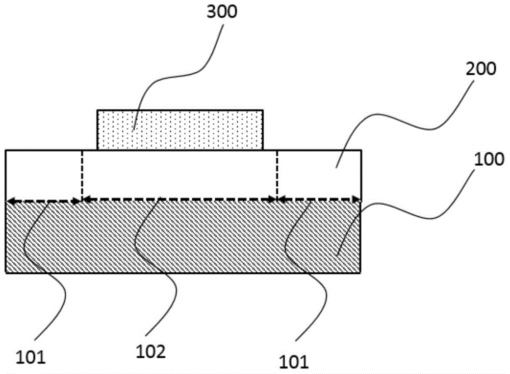
[0033] The flexible film substrate and substrate separation process for the preparation of flexible display devices in this embodiment includes the following steps:

[0034] (1) if figure 1 As shown, the flexible film substrate 200 is prepared on the carrier substrate 100, and differential treatment is performed on the joint between the flexible film substrate 200 and the carrier substrate 100, so that there is a gap between the flexible film substrate 200 and the carrier substrate 100 in some areas. The adhesion force between the flexible film substrate and the carrier substrate in other areas is 0 dB or 1 dB, forming a low adhesion area 102 . dB is the unit of action for expressing adhesion in the industry. The standard is formulated by ASTM, and an integer from 0 to 5 is used to represent the magnitude of adhesion, of which 5 represents the highest adhesion, and 0 corresponds to no adhesion.

[0035] In this embodiment, differential treatment is performed on the joint betw...

Embodiment 2

[0046] The flexible thin film substrate and substrate separation process for the preparation of flexible display devices in this embodiment, other features are the same as in embodiment 1, the difference lies in the joint between the flexible thin film substrate and the carrier substrate in step (1) Differentiated processing is carried out in the following ways:

[0047] After the flexible film substrate 200 is prepared on the carrier substrate 100, on the flexible film substrate 200 above the high-adhesion region 101 to be formed, a high-temperature, high-pressure heat treatment is performed with a thermal probe, such as Figure 5 shown.

[0048] In this embodiment, after the flexible film substrate is heat-treated, the molecular chains of the polymer flexible film substrate begin to move in the vicinity of the glass transition temperature (350°C-500°C), and the side reaction phenomenon is intensified, such as the hydroxyl group on the polyimide Forms covalent bonds with the...

Embodiment 3

[0051] The flexible thin film substrate and substrate separation process for the preparation of flexible display devices in this embodiment, other features are the same as in embodiment 1, the difference lies in the joint between the flexible thin film substrate and the carrier substrate in step (1) Differentiated processing is carried out in the following ways:

[0052] Before preparing the flexible thin film substrate 200, the bonding layer 400 is sputtered on some regions of the surface of the carrier substrate 100, so that these regions become high adhesion regions 101 after the flexible thin film substrate is prepared, such as Figure 6 shown.

[0053] The thickness of the bonding layer is between 1 and 300 microns, and the specific material is a metal film, which can be aluminum, titanium or molybdenum metal film; the bonding layer can also be a metal oxide film, which can be aluminum oxide, indium zinc oxide or copper oxide film. The bonding layer can be deposited as ...


PUM

PropertyMeasurementUnit
Thicknessaaaaaaaaaa
Thicknessaaaaaaaaaa
The average thicknessaaaaaaaaaa

Abstract

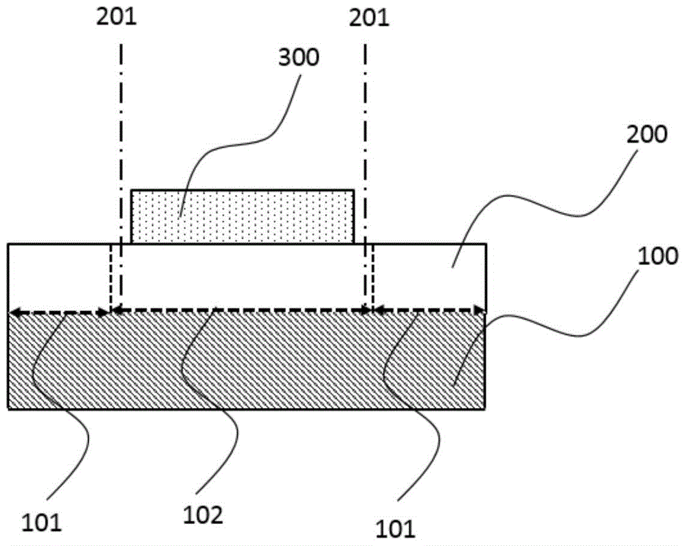
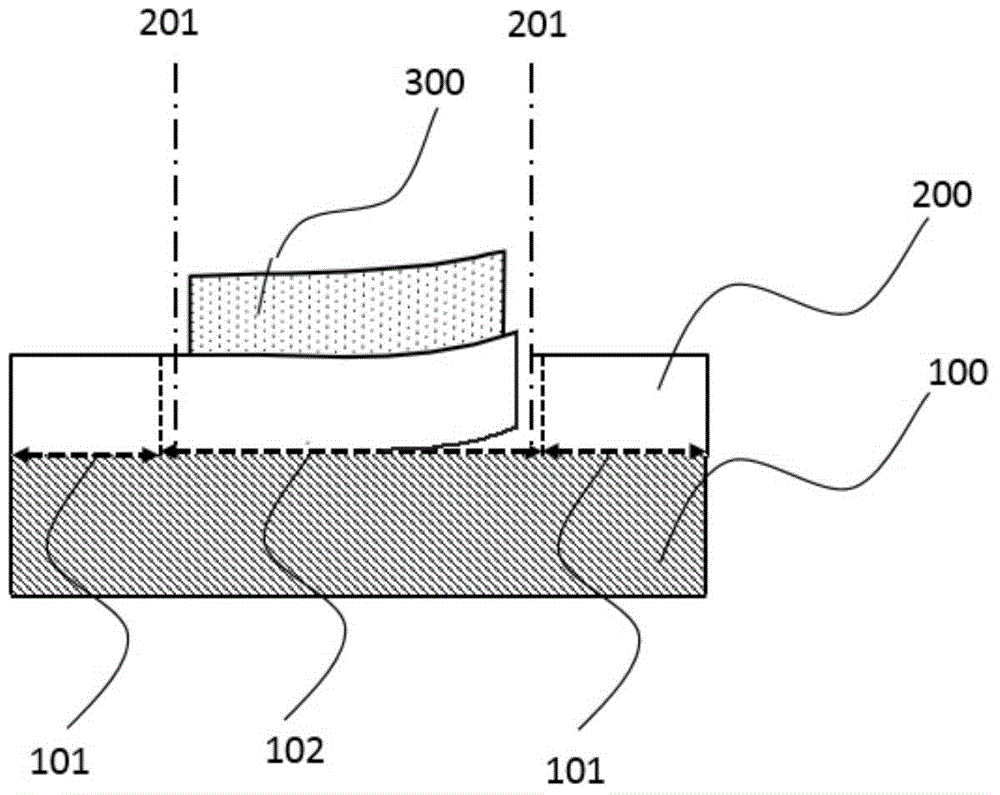
The invention discloses a flexible membrane liner and substrate separation process for producing a flexible display device. The process includes the steps: (1) producing a flexible membrane liner on a carrier substrate, and treating the juncture of the flexible membrane liner and the carrier substrate to enable some regions to become high-adhesion regions and the rest region to become a low-adhesion region; (2) producing an electronic component on the flexible membrane liner over the low-adhesion region; (3) cutting vertically and downwardly from the flexible membrane liner along the periphery of the electronic component to form a cutting line, wherein the low-adhesion region is located under the cutting line; (4) separating the flexible membrane liner from the carrier substrate. The flexible membrane liner is stably attached to the carrier substrate in the subsequent device production process, and the process is simple in liner and substrate separation, low in cost and rapid and causes no damage to the device.

Description

technical field [0001] The invention relates to the field of preparation of flexible display devices, in particular to a process for separating a flexible film substrate and a substrate for the preparation of flexible display devices. Background technique [0002] In the preparation of flexible display devices, a flexible thin film substrate is first formed on a hard substrate, and then electronic devices are fabricated on the flexible thin film substrate, and finally the flexible thin film substrate is separated from the substrate to obtain a finished device without the substrate. However, this method in the prior art has some defects: flexible substrates and substrates need to withstand harsh experimental conditions such as ion bombardment, chemical corrosion, ultraviolet radiation, and high-temperature treatment during the subsequent preparation of electronic devices, resulting in the substrate The adhesion between the substrate and the substrate is greatly improved, and ...

Claims


Application Information

Patent Timeline
IPC IPC(8): H01L51/56
CPCH10K71/00H10K77/111Y02E10/549Y02P70/50
Inventor 王磊许志平徐苗李洪濛邹建华陶洪彭俊彪
Owner SOUTH CHINA UNIV OF TECH
Learn More