Semiconductor packaging method of wafer level silicon-based through hole

A packaging method and a technology of through-silicon vias, which are applied in semiconductor devices, semiconductor/solid-state device manufacturing, and electrical solid-state devices, etc., can solve problems such as easy generation of fragments, slivers, accelerated device failure, and affect product reliability, etc., to reduce challenges , Reduce the overall size and realize the effect of miniaturization

Inactive Publication Date: 2015-03-04
BEIJING UNIV OF TECH
View PDF4 Cites 28 Cited by
  • Summary
  • Abstract
  • Description
  • Claims
  • Application Information

AI Technical Summary

Problems solved by technology

[0005] However, in current semiconductor packaging products, especially for packaging types such as wafer-level image sensors, MEMS devices, and integrated chips, there are still many problems that affect product reliability:
Since the area to be cut contains a variety of materials with different hardness, such as redistribution circuit layer, silicon, polymer, cover plate 101, etc., this poses a great challenge to the cutting process, and it is easy to generate fragments, slivers, etc.
On the other hand, during the subsequent service of the packaged product, since the metal layer 108 is in direct contact with the outside world around the package structure, once delamination occurs between the interfaces, it is easy to introduce moisture from the external environment into the package structure. , resulting in accelerated failure of the device

Method used


Image

  • Semiconductor packaging method of wafer level silicon-based through hole
  • Semiconductor packaging method of wafer level silicon-based through hole
  • Semiconductor packaging method of wafer level silicon-based through hole

Examples


Embodiment Construction

[0036] The present invention will be described in more detail below with reference to accompanying drawing:

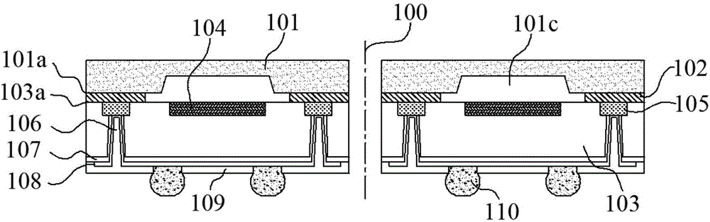
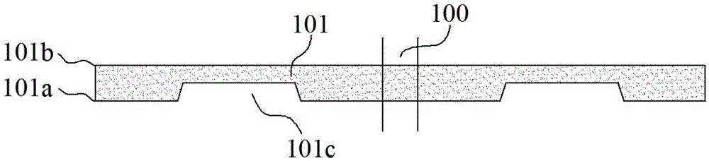
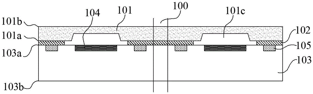
[0037] by figure 1As shown, the wafer-level semiconductor package containing through-silicon vias according to the embodiment of the present invention includes: 1. a cover plate 101, and a cavity structure 101c is fabricated on the front surface 101a of the cover plate; 2. a wafer 103, which includes a wafer Circular front 103a and wafer back 103b; 3. functional area 104 and bonding pads 105, a plurality of chip areas are prefabricated on the wafer front 103a, each chip area includes a central functional area 104 and several bonding pads 105 around ; 4. Bonding glue 102, by coating a layer of bonding glue 102 on the front surface 101a of the cover plate, bonding the front surface 101a of the cover plate with the front surface 103a of the wafer; 103b making through-silicon vias 106 to expose the pads 105 for connection to the subsequent redistribution circuit layer; 6....


PUM


Abstract

The invention discloses a semiconductor packaging method of wafer level silicon-based through hole, belonging to the field of semiconductor packaging. The packaging method substantially comprises the following steps: 1, making a cavity structure on a cover plate; 2, bonding the front surface of the cover plate with the front surface of a wafer through a bonding machine; 3, grinding the rear surface of the wafer by a grinder, and implementing a stress plasma etching on the rear surface of the wafer; 4, removing all silicon belonging to a scribe line region starting from the rear surface of the wafer; 5, etching the rear surface of the wafer in order to form silicon through holes, and exposing a bonding pad; 6, making passivation layers, metal layers and solder mask layers sequentially in the rear surface of the wafer and the silicon through holes, so as to compose a redistributed circuit layer, thereby conducting the solder pad to a designated solder ball position on the rear surface of the wafer; 7, making solder balls and cutting along the scribe line. By the implementation of the semiconductor packaging method of wafer level silicon-based through hole, the yield rate of wafer cutting technique is increased, the stress level in package structure is reduced, and the boundary dimension of the package structure is decreased.

Description

technical field [0001] The invention relates to the field of semiconductor packaging, in particular to a wafer-level semiconductor packaging method containing through-silicon holes. The method can be preferably used in image sensors, MEMS devices or integrated chips and the like. Background technique [0002] With the rapid development of electronic technology, personal consumer electronic products such as mobile phones and notebook computers are also developing in the direction of lighter, thinner, faster and more portable. The packaging form of semiconductor chips has also gone through metal circular packaging (TO), small outline packaging (SOP), quad flat packaging (QFP), solder ball array packaging (BGA) to multi-chip and system-level three-dimensional packaging. The ratio of the chip area to the package area is getting closer or even exceeding 1, the number of pins is increasing, and the reliability is getting better and better. [0003] Wafer level packaging (WLP) is...

Claims


Application Information

Patent Timeline
Patent Type & Authority Applications(China)
IPC IPC(8): H01L21/768H01L21/56
CPCH01L21/561H01L21/76898H01L2224/11H01L2924/16235
Inventor 秦飞武伟安彤肖智轶
Owner BEIJING UNIV OF TECH
Why Eureka
Try Eureka