Supercharge Your Innovation With Domain-Expert AI Agents!

Insert layer composite structure and manufacturing method thereof

A composite structure and intercalation layer technology, applied in semiconductor/solid-state device manufacturing, semiconductor devices, electrical components, etc., can solve the problem of poor repeatability of ohmic contact resistivity, low ohmic contact resistivity, poor current expansion, etc. problem, to achieve the effect of increasing the carrier concentration, reducing the specific contact resistivity, and uniforming the current transport

Active Publication Date: 2015-03-04
INST OF MICROELECTRONICS CHINESE ACAD OF SCI
View PDF3 Cites 6 Cited by
  • Summary
  • Abstract
  • Description
  • Claims
  • Application Information

AI Technical Summary

Problems solved by technology

However, if the metal is too thin, the current spreadability will be poor, which will make the repeatability of the ohmic contact resistivity measurement worse, the device stability will not be strong, and it is impossible to form a lower ohmic contact resistance on the wide bandgap semiconductor material at the same time Rate

Method used


Image

  • Insert layer composite structure and manufacturing method thereof
  • Insert layer composite structure and manufacturing method thereof
  • Insert layer composite structure and manufacturing method thereof

Examples


Embodiment Construction

[0029] The following will clearly and completely describe the technical solutions in the embodiments of the present invention with reference to the accompanying drawings in the embodiments of the present invention. Obviously, the described embodiments are only some, not all, embodiments of the present invention. Based on the embodiments of the present invention, all other embodiments obtained by persons of ordinary skill in the art without making creative efforts belong to the protection scope of the present invention.

[0030] In order to make the object, technical solution and advantages of the present invention clearer, the present invention will be described in further detail below in conjunction with specific embodiments and with reference to the accompanying drawings.

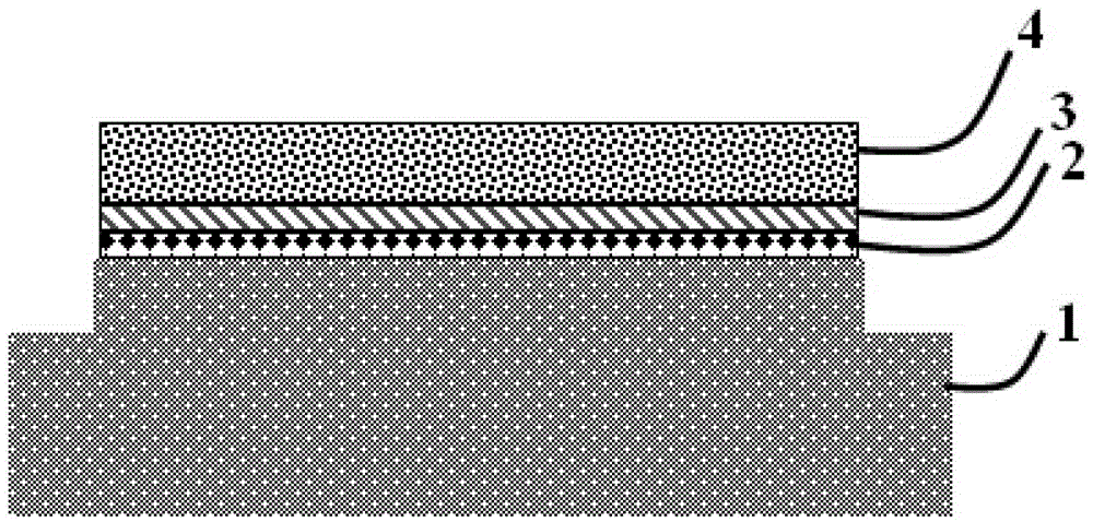
[0031] An embodiment of the present invention provides an insertion layer composite structure, such as figure 1 As shown, the intercalation layer composite structure is located between the SiC substrate 1...


PUM

PropertyMeasurementUnit
Thicknessaaaaaaaaaa
Total thicknessaaaaaaaaaa
Thicknessaaaaaaaaaa

Abstract

The invention discloses an insert layer composite structure and a manufacturing method thereof, relates to the technical field of large energy gap material ohmic contact formation, and solves the problems of poor ohmic contact resistivity measuring repeatability, low device stability, difficult ohmic contact formation on large energy gap semiconductor materials and high ohmic contact resistivity in the prior art. The insert layer composite structure is positioned between a SiC substrate and a metal cover layer and comprises a current transport layer and an ohmic contact metal layer, the current transport layer is made of special materials, the ohmic contact metal layer has a specific element component ratio, the current transport layer is positioned on the SiC substrate, and the ohmic contact metal layer is positioned above the current transport layer. The ohmic contact metal layer enters the current transport layer through diffusion of carbide and silicide and is mixed with the current transport layer to form the insert layer composite structure, wherein the carbide and the silicide are formed by an alloy annealing mode and have a specific chemical component ratio. The insert layer composite structure is applicable to simultaneously forming P-type and N-type ohmic contact on the large energy gap semiconductor materials or individually forming P-type or N-type ohmic contact.

Description

technical field [0001] The invention relates to the technical field of forming ohmic contacts with wide bandgap materials, in particular to an insertion layer composite structure and a manufacturing method thereof. Background technique [0002] Obtaining good ohmic contact quality of wide-bandgap silicon carbide (SiC) materials is a key factor for realizing high-temperature, high-voltage, high-frequency and high-power applications of SiC devices. Especially for SiC metal oxide field effect transistor (MOSFET) devices, it is required to form ohmic contacts in the n+ source region and p well region at the same time. In order to ensure the quality of the MOSFET gate oxide layer surface, the requirements for the ohmic contact metal system and alloy annealing conditions At the same time, due to the influence of factors such as high temperature activation annealing and alloy annealing, the quality of contact surface morphology and interface microstructure also have a great impact ...

Claims


Application Information

Patent Timeline
IPC IPC(8): H01L29/45H01L21/04
CPCH01L21/0485H01L29/45
Inventor 汤益丹申华军白云周静涛杨成樾刘新宇
Owner INST OF MICROELECTRONICS CHINESE ACAD OF SCI
Features
  • R&D
  • Intellectual Property
  • Life Sciences
  • Materials
  • Tech Scout
  • Unparalleled Data Quality
  • Higher Quality Content
  • 60% Fewer Hallucinations
Learn More