A kind of nitride led epitaxial structure using sic substrate and preparation method thereof
A technology of nitride epitaxial layer and epitaxial structure, which is applied in the direction of electrical components, circuits, semiconductor devices, etc., can solve the problems of expensive equipment, many process parameters, and poor process consistency, and achieve simplified stripping process, high crystal quality, and improved good quality. rate effect
- Summary
- Abstract
- Description
- Claims
- Application Information
AI Technical Summary
Problems solved by technology
Method used
Image

Examples
preparation example Construction
[0059] The preparation of the two-dimensional derivative film is directly grown on the SiC substrate by the method of high temperature annealing or chemical vapor deposition or physical vapor deposition; the preparation method of the nitride epitaxial layer includes organic metal chemical vapor deposition , at least one of radio frequency magnetron sputtering, molecular beam epitaxy, pulsed laser deposition or hydride vapor phase epitaxy; wherein,
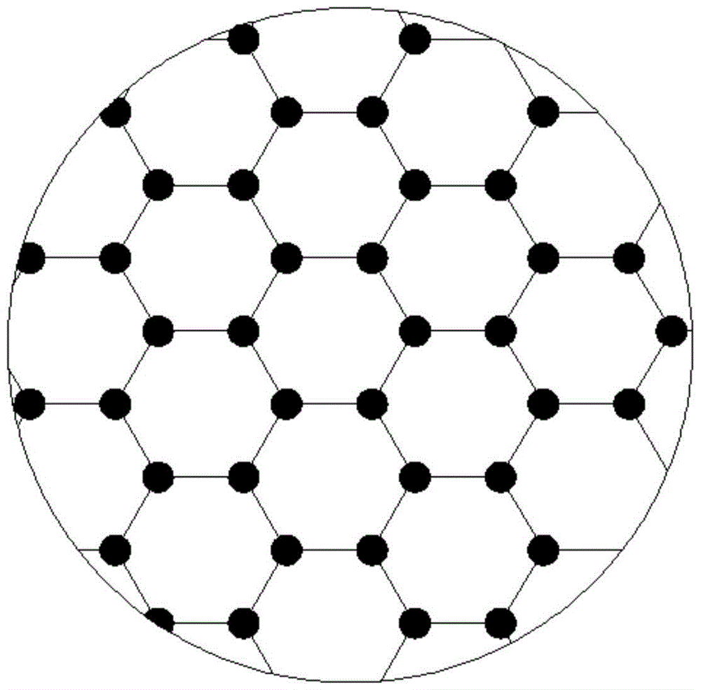
[0060] Described graphene is to make by the method for high temperature annealing or the method for chemical vapor deposition:
[0061] The specific steps of the high-temperature annealing method are as follows: place the SiC substrate at a temperature of 1500-2000°C and a vacuum degree of ≤10 -3 In the environment of Pa, or the temperature is 1300~1800℃, the pressure is ≥10 2 In the environment of argon atmosphere of Pa, graphitization is realized through the sublimation of silicon atoms on the surface of the substrate to obtain ...
Embodiment 1
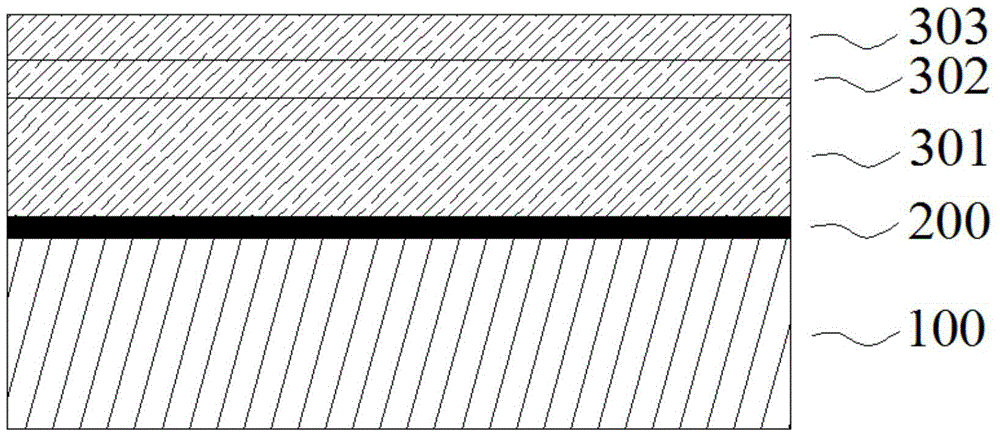
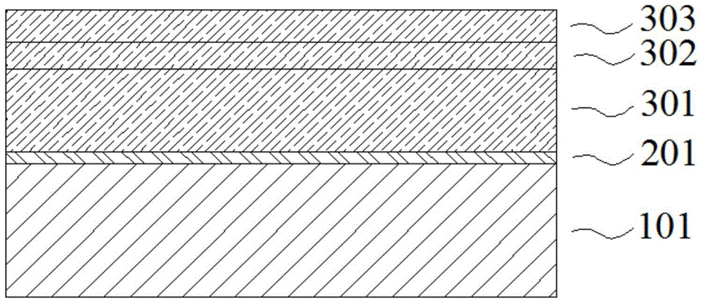
[0076] Such as image 3 As shown, a single-layer graphene 201 is fabricated on the surface of a 4H-SiC substrate 101 as a two-dimensional derivative film, and then a nitride blue LED epitaxial layer is grown thereon. Wherein, the structural parameters of the n-type electron injection layer 301 are as follows: a 2 μm thick n-type GaN layer, the doping element is Si, and the doping concentration is 1.0×10 19 ; The structural parameters of the active layer 302 are as follows: In 0.15 Ga 0.85 N / GaN multiple quantum well light-emitting layer, In 0.15 Ga 0.85 The single-layer thicknesses of N and GaN are 3nm and 10nm respectively, and the number of periods of the multiple quantum wells is 5; the structural parameters of the p-type hole injection layer 303 are as follows: it includes two sublayers, one is a p-type GaN layer with a thickness of 0.2 μm, The p-type doping element is Mg, and the doping concentration is 1.0×10 20 ; the other is a 10nm thick p-type heavily doped p ++...
Embodiment 2
[0080] Such as Figure 4 As shown, a multi-layer hexagonal boron nitride (h-BN) derivative film 202 is fabricated on the surface of a 6H-SiC substrate 102 as a two-dimensional derivative film, and then a nitride green LED epitaxial layer is grown thereon. Wherein, the structural parameters of the n-type electron injection layer 301 are as follows: a 2 μm thick n-type GaN layer, the doping element is Si, and the doping concentration is 1.0×10 19 ; The structural parameters of the active layer 302 are as follows: In 0.3 Ga 0.7 N / GaN multiple quantum well light-emitting layer, In 0.3 Ga 0.7 The single-layer thicknesses of N and GaN are 2nm and 10nm respectively, and the period number of the multiple quantum wells is 4; the structural parameters of the p-type hole injection layer 303 are as follows: it includes two sublayers, one is a p-type GaN layer with a thickness of 0.2 μm, The p-type doping element is Mg, and the doping concentration is 1.0×10 20 ; the other is a 10nm t...
PUM
| Property | Measurement | Unit |
|---|---|---|
| thickness | aaaaa | aaaaa |
| thickness | aaaaa | aaaaa |
| thickness | aaaaa | aaaaa |
Abstract
Description
Claims
Application Information