Right-angle gate field plate HFET (Heterojunction Field Effect Transistor) and manufacturing method thereof

A heterojunction field effect and transistor technology, applied in semiconductor/solid-state device manufacturing, semiconductor devices, electrical components, etc., can solve the problems of reducing device yield, cumbersome process debugging, increasing device difficulty, etc., to improve reliability, The effect of reducing the electric field and reducing the gate leakage current

Active Publication Date: 2015-03-11
XIDIAN UNIV
View PDF4 Cites 2 Cited by
  • Summary
  • Abstract
  • Description
  • Claims
  • Application Information

AI Technical Summary

Problems solved by technology

However, the process of GaN-based double-layer field plate HEMT devices is complex and the manufacturing cost is higher. The fabrication of each field plate requires process steps such as photolithography, metal deposition, and passivation dielectric deposition.
Moreover, in order to optimize the thickness of the dielectric material under the field plates of each layer to maximize the breakdown voltage, tedious process debugging and optimization must be carried out, which greatly increases the difficulty of device manufacturing and reduces the yield of devices.

Method used


Image

  • Right-angle gate field plate HFET (Heterojunction Field Effect Transistor) and manufacturing method thereof
  • Right-angle gate field plate HFET (Heterojunction Field Effect Transistor) and manufacturing method thereof
  • Right-angle gate field plate HFET (Heterojunction Field Effect Transistor) and manufacturing method thereof

Examples


Embodiment 1

[0038] Embodiment one: making substrate is sapphire, and passivation layer is Al 2 o 3 , the protective layer is SiO 2 , the right-angle gate field plate is a right-angle gate field plate heterojunction field effect transistor of Ti / Mo / Au metal combination.

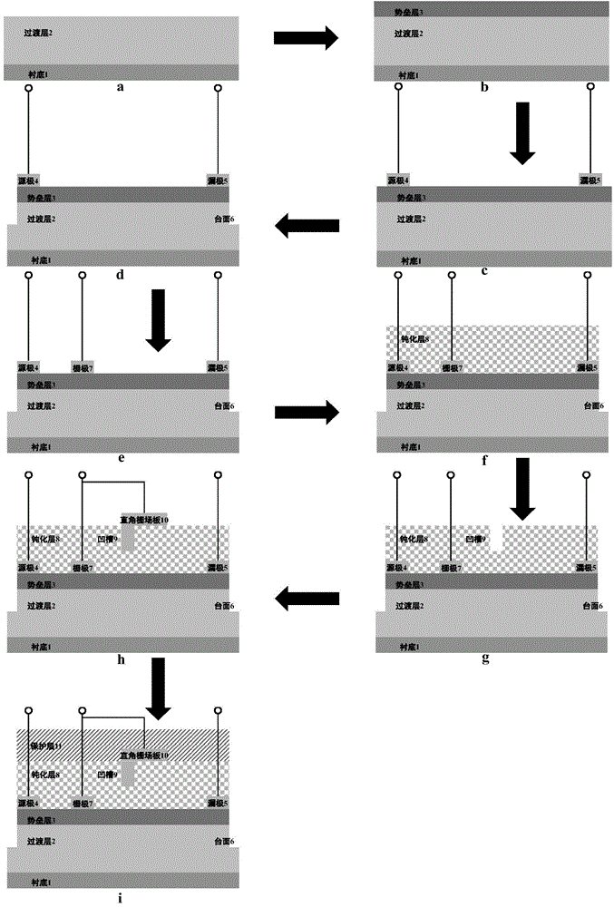
[0039] Step 1. On the sapphire substrate 1, make the transition layer 2 by epitaxial GaN material from bottom to top, such as image 3 a.

[0040] An undoped transition layer 2 with a thickness of 1 μm is epitaxially formed on the sapphire substrate 1 by metal organic chemical vapor deposition technology, and the transition layer is composed of GaN materials with thicknesses of 30 nm and 0.97 μm from bottom to top. The process conditions used for the epitaxial lower layer GaN material are: temperature 530°C, pressure 45 Torr, hydrogen gas flow rate 4400 sccm, ammonia gas flow rate 4400 sccm, gallium source flow rate 22 μmol / min; the process conditions for the epitaxial upper layer GaN material are: temperature 960°C, ...

Embodiment 2

[0057] Embodiment 2: The substrate is made of silicon carbide, and the passivation layer is SiO 2 , the protective layer is SiN, and the right-angle gate field plate is a right-angle gate field plate heterojunction field effect transistor composed of Ti / Ni / Au metal.

[0058] Step 1. Epitaxially AlN and GaN materials on the silicon carbide substrate 1 to form the transition layer 2, such as image 3 a.

[0059] 1.1) Using metal-organic chemical vapor deposition technology to epitaxially undoped AlN material with a thickness of 50nm on the silicon carbide substrate 1; the process conditions for the epitaxy are: temperature is 1000°C, pressure is 45Torr, hydrogen flow rate is 4600sccm, The flow rate of ammonia gas is 4600 sccm, and the flow rate of aluminum source is 5 μmol / min;

[0060] 1.2) Using metal-organic chemical vapor deposition technology to epitaxially GaN material with a thickness of 2.45 μm on the AlN material to complete the fabrication of the transition layer 2; ...

Embodiment 3

[0088] Embodiment three: making substrate is silicon, and passivation layer is SiN, and protection layer is SiO 2 , the right-angle gate field plate is a right-angle gate field plate heterojunction field effect transistor composed of Ti / Pt / Au metal.

[0089] Step A. Epitaxial AlN and GaN materials on the silicon substrate 1 from bottom to top to make the transition layer 2, such as image 3 a.

[0090] A1) Using metal-organic chemical vapor deposition technology at a temperature of 800° C., a pressure of 40 Torr, a flow rate of hydrogen gas of 4000 sccm, a flow rate of ammonia gas of 4000 sccm, and a flow rate of aluminum source of 25 μmol / min, the epitaxy on the silicon substrate 1 AlN material with a thickness of 200nm;

[0091] A2) Using metal-organic chemical vapor deposition technology at a temperature of 980°C, a pressure of 45 Torr, a flow rate of hydrogen gas of 4000 sccm, a flow rate of ammonia gas of 4000 sccm, and a flow rate of gallium source of 120 μmol / min, the...


PUM

PropertyMeasurementUnit
Depthaaaaaaaaaa
Widthaaaaaaaaaa
Thicknessaaaaaaaaaa

Abstract

The invention discloses a right-angle gate field plate HFET (Heterojunction Field Effect Transistor) and a manufacturing method thereof and mainly solves the problem of complex processes of high breakdown voltage achievement in the prior art of field plates. The right-angle gate field plate HFET comprises a substrate (1), a transition layer (2), a barrier layer (3), a source electrode (4), a drain electrode (5), a mesa (6), a gate electrode (7), a passivating layer (8) and a protection layer (11), wherein a groove (9) is arranged inside the passivating layer (8), a right-angle gate field plate (10) is deposited between the passivating layer (8) and the protection layer (11), the edge of the side of the right-angle gate field plate (10), which is close to the gate electrode, is level with the edge of the side of the groove, which is close to the gate electrode, the right-angle gate field plate is electrically connected with the gate electrode (7), and the lower end of the right-angle gate field plate is completed filled inside the groove (9). The right-angle gate field plate HFET has the advantages of simple process and high breakdown voltage, field plate efficiency, reliability and finished product rate.

Description

technical field [0001] The invention belongs to the technical field of semiconductor devices, in particular to a right-angle gate field plate heterojunction field effect transistor, which can be used as a basic device of a power electronic system. technical background [0002] Power semiconductor devices are important components of power electronic systems and effective tools for power processing. In recent years, as energy and environmental issues have become increasingly prominent, research and development of new high-performance, low-loss power devices has become one of the effective ways to improve power utilization, save energy, and alleviate energy crises. However, in the research of power devices, there is a serious constraint relationship between high speed, high voltage and low on-resistance. Reasonable and effective improvement of this constraint relationship is the key to improving the overall performance of the device. As the market continues to put forward high...

Claims


Application Information

Patent Timeline
IPC IPC(8): H01L29/778H01L29/423H01L29/06H01L21/335
CPCH01L29/06H01L29/402H01L29/66431H01L29/778
Inventor 毛维郝跃范举胜董萌刘红侠杨林安王冲郑雪峰张金风
Owner XIDIAN UNIV
Why Eureka
Try Eureka