Chip-integrated 2-micrometer wavelength micro laser
A micro-laser, laser technology, applied in lasers, laser parts, phonon exciters, etc., can solve the problem that no one has developed a micro-laser, and achieve the effect of optimizing the energy mode volume, low threshold and high quality
- Summary
- Abstract
- Description
- Claims
- Application Information
AI Technical Summary
Problems solved by technology
Method used
Image
Examples
preparation example Construction
[0039] The preparation process of the 2 micron wavelength laser of the present invention is as follows:
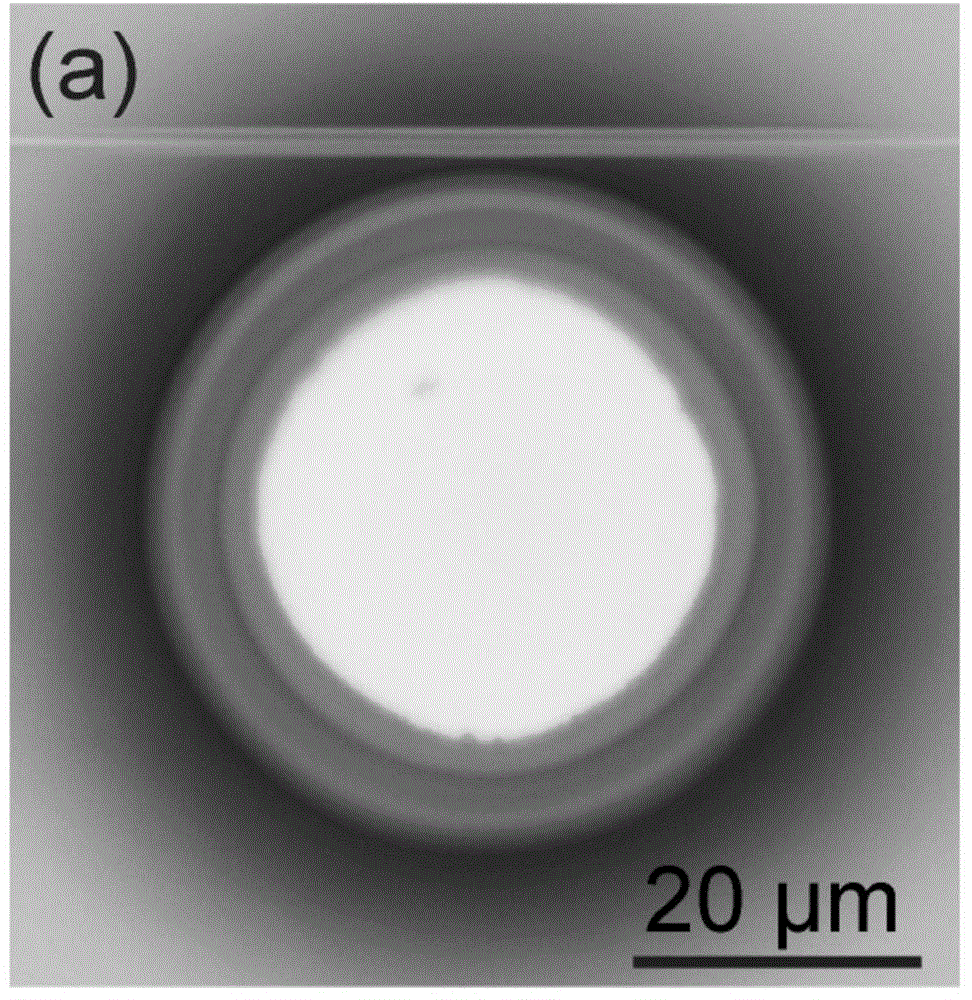
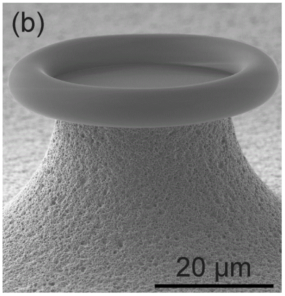
[0040] (1) Firstly, prepare rare earth-doped silicon oxide film by sol-gel method, the film thickness is 1 micron ~ 2 micron; (2) After using photolithography, wet etching and dry etching, the silicon oxide microdisk cavity is obtained (3) Use a carbon dioxide laser to heat and reflow the silicon oxide microdisk cavity, where the power of the carbon dioxide laser is 7-10W, and the heating and reflow treatment time is 25 to 35 seconds to melt the silicon oxide microdisk cavity into silicon oxide microrings Core cavity. Specifically, using a carbon dioxide laser to heat and reflow the silicon oxide microdisk includes the following steps: first irradiate the surface of the silicon oxide microdisk cavity with a first power laser for 10-15 seconds to obtain an initial state silicon oxide microring core cavity, Then the surface of the initial state microring core cavity is irradia...
Embodiment 1
[0042] A doped silicon oxide film with a thickness of 1.35 microns was obtained by the sol-gel method, and the concentration of thulium ions was 1×10. 19 cm -3 , 2×10 19 cm -3 , 4×10 19 cm -3 . After photolithography, wet etching and dry etching, a silicon oxide microdisc cavity is obtained. A carbon dioxide laser is used to heat and reflow the silicon oxide microdisk cavity to obtain a silicon oxide microring core cavity. On the other hand, the high-temperature drawing method is used to draw ordinary single-mode optical fibers into micro-nano optical fibers with a diameter of 1 to 2 microns. Then put the silicon oxide microring core cavity on the three-dimensional piezoelectric console, precisely control its position, slowly bring the two closer together, and input the adjustable continuous pump light of the 1.6 micron band from the fiber end A. When the micro-nano fiber and the micro-ring core cavity are at the best coupling point, the energy will be absorbed by the micro...
Embodiment 2
[0044] A doped silicon oxide film with a thickness of 1.35 microns was obtained by the sol-gel method, in which the concentration of thulium ions was 2.6×10 19 cm -3 , 3.3×10 19 cm -3 , 4×10 19 cm -3 , The concentration of holmium ion doped is 5×10 18 cm -3 . The concentration ratio of thulium ion and holmium ion is 5.2, 6.6, and 8, respectively. Then through photolithography, etching and carbon dioxide laser reflow process, a thulium-holmium co-doped silicon oxide microring core cavity is obtained. At the same time, a micro-nano fiber with a diameter of 1 μm to 2 μm is prepared by the high-temperature drawing method. Then the coupling between the silicon oxide micro-ring core cavity and the micro-nano fiber is precisely controlled, and at the same time, the adjustable continuous pump light in the 1.6 micron band is input from the fiber A end. As the power of the pump light increases, rare earth ions will produce fluorescence. At the same time, thulium ions will absorb th...
PUM
| Property | Measurement | Unit |
|---|---|---|
| wavelength | aaaaa | aaaaa |
| diameter | aaaaa | aaaaa |
| diameter | aaaaa | aaaaa |
Abstract
Description
Claims
Application Information


