Preparation method of ZnO-based dilute magnetic semiconductor film and its in-situ regulation method of charge concentration
A dilute magnetic semiconductor, zinc oxide-based technology, used in semiconductor/solid-state device manufacturing, circuits, electrical components, etc., can solve the problems of depositing dilute magnetic semiconductor films, maintaining consistency, and difficult to obtain physical properties of dilute magnetic semiconductor films.
- Summary
- Abstract
- Description
- Claims
- Application Information
AI Technical Summary
Problems solved by technology
Method used
Image
Examples
preparation example Construction
[0034] The preparation method includes: high-purity Zn 1-x mn x The O ceramic block is used as the target, and pulsed laser deposition is performed on a single-sided polished (111) PMN-x′PT single crystal substrate to obtain the Zn 1-x mn x O thin film, wherein the parameters of the pulsed laser deposition technology are: put the single-side polished (111) oriented PMN-x′PT substrate into the reaction chamber of the pulsed laser deposition system, and extract the background of the pulsed laser deposition system Vacuum to ≦5×10 -4 Pa, heat the substrate to 500~600°C, then vacuum the reaction chamber to ≦5×10 -4 Pa; with high purity Zn 1-x mn x O ceramic target is used as the target material, the deposition temperature is 400-750°C, the deposition oxygen pressure is 0.001-1Pa, and the laser energy is 2-6J / cm 2 , deposition rate 1 ~ 5nm / min.
[0035] The high-purity Zn 1-x mn x The purity of O ceramic blocks is greater than 99.99%.
[0036] The purity of the deposited o...
Embodiment 1
[0049] (1) Film preparation: use high-purity (≥99.99%) Zn 0.95 mn 0.05 O ceramic block as the target, the (111) orientation 0.71PbMg polished on one side 1 / 3 Nb 2 / 3 o 3 -0.29PbTiO 3 (PMN-29PT) is placed in the reaction chamber of the pulsed laser deposition device, the background vacuum is pumped to ≦5×10⁻⁴Pa, the substrate is heated to 600°C, and the vacuum is pumped to 4×10 -4 Pa; with high purity (≥99.999%) O 2 As a reaction gas, the pressure of the reaction chamber is 0.01Pa, and the laser energy is 5J / cm 2 , the distance between substrate and target is 7cm, and thin film deposition is carried out to obtain Zn 0.95 mn 0.05 O film (here, we approximately think that the content of Mn element in the film is the same as that of the ceramic block);
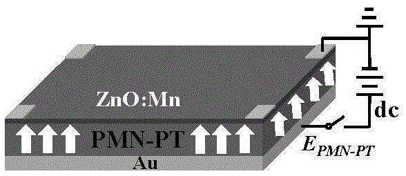
[0050] (2) Electrode preparation: in Zn 0.95 mn 0.05 Gold electrodes were sputtered on the surface of the O film and the back of the PMN-29PT substrate. get as figure 1 the structure shown;
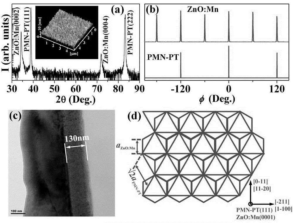
[0051] (3) Structural char...
Embodiment 2
[0056] (1) The preparation process is basically the same as in Example 1, except that the deposition oxygen pressure is 0.1Pa;
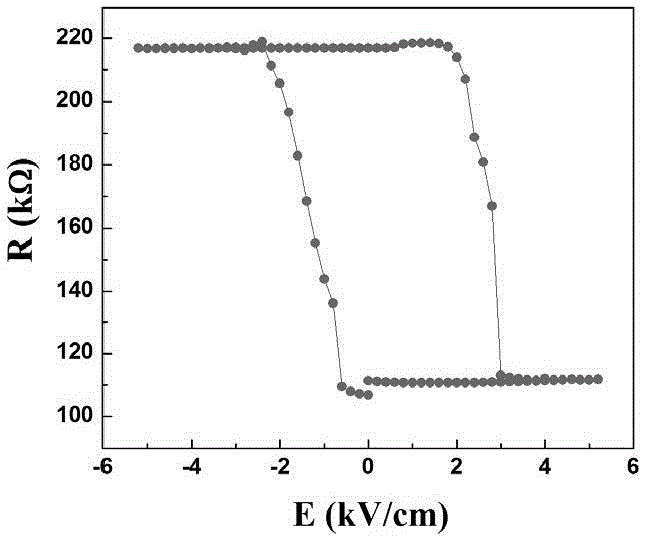
[0057] (2) Figure 5 For the prepared Zn of embodiment 2 0.95 mn 0.05 The change curve of O sheet resistance with the bipolar voltage applied on the PMN-29PT substrate is also a square shape consistent with the hysteresis loop of PMN-29PT, and the coupling mechanism of the system is the interface charge effect. The relative change of sheet resistance caused by polarization reversal of PMN-29PT substrate at room temperature is 100%;
[0058](3) Hall effect measurement result shows that the Zn prepared by embodiment 2 0.95 mn 0.05 The carrier type of O film is n-type, and the carrier concentration at room temperature is about 2.5×10 18 / cm 3 .
PUM
| Property | Measurement | Unit |
|---|---|---|
| thickness | aaaaa | aaaaa |
| surface roughness | aaaaa | aaaaa |
| thickness | aaaaa | aaaaa |
Abstract
Description
Claims
Application Information


