Rectifier and manufacturing method thereof

A manufacturing method and rectifier technology, which are applied in semiconductor/solid-state device manufacturing, electric solid-state devices, semiconductor devices, etc., can solve the problems of reducing the forward voltage drop of the device, limiting the channel density, limiting the cost of the device, etc., so as to reduce the positive voltage. Effects of conduction voltage drop, low manufacturing cost, and increased channel density

Active Publication Date: 2015-04-15
CSMC TECH FAB2 CO LTD
View PDF13 Cites 2 Cited by
  • Summary
  • Abstract
  • Description
  • Claims
  • Application Information

AI Technical Summary

Problems solved by technology

First, there is a parasitic JFET (junction gate field-effect transistor) resistance between the two channels, which limits the forward voltage drop of the device to further reduce
In addition, the planar structure greatly limits the channel density of Channel Diode per unit area, thus limiting the space for device cost reduction

Method used


Image

  • Rectifier and manufacturing method thereof
  • Rectifier and manufacturing method thereof
  • Rectifier and manufacturing method thereof

Examples


Embodiment 1

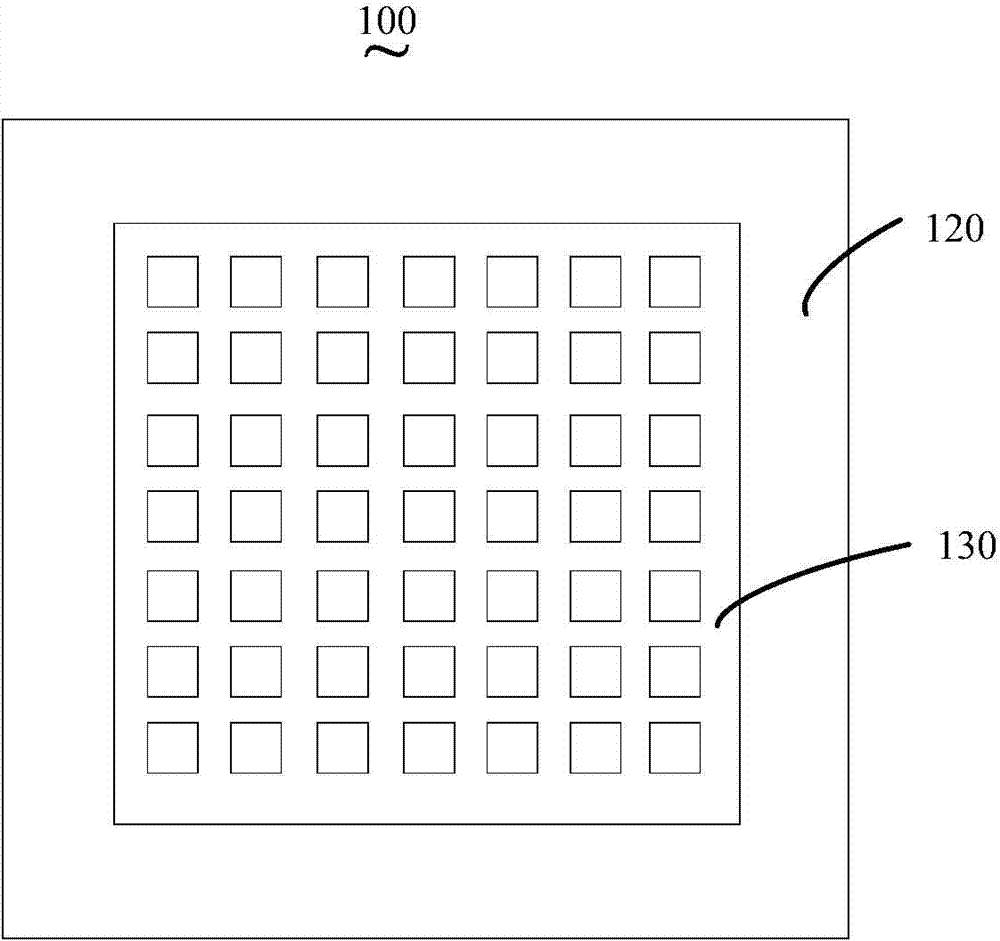
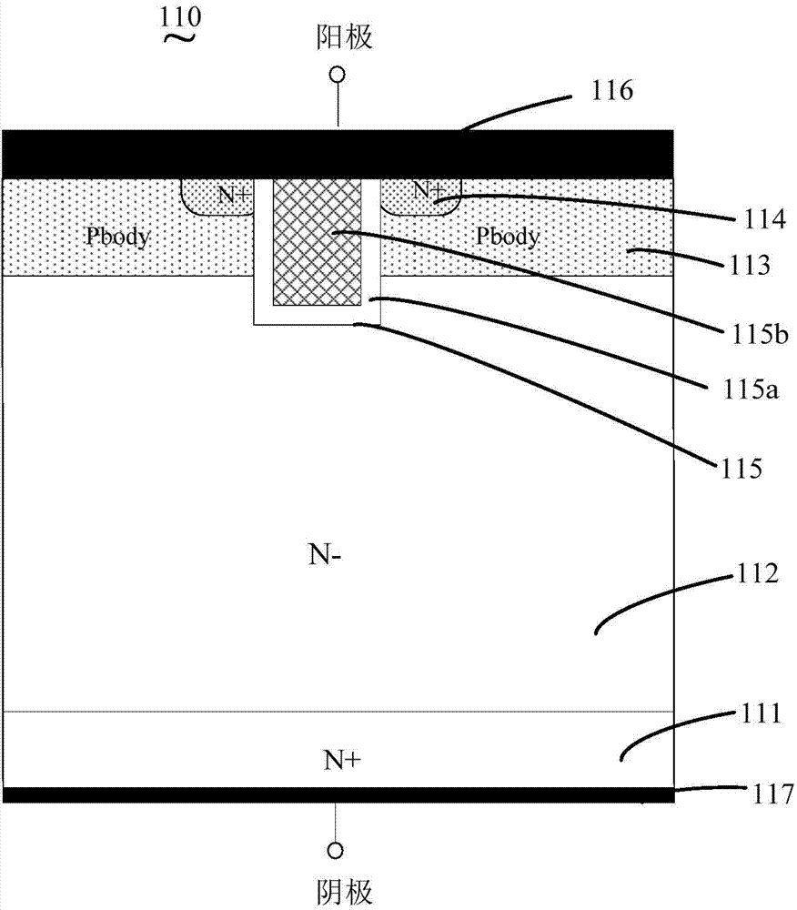
[0024] Please refer to figure 1 and figure 2 , an embodiment provides a rectifier 100 . The rectifier 100 includes a cell region 130 and a guard ring region 120 around the cell region 130 . The cell region 130 includes a plurality of rectifier diodes 110 . The guard ring area 120 includes a plurality of guard rings, and the guard rings can function to improve the withstand voltage of the rectifier 100 . Among them, refer to figure 2 , the rectifier diode 110 includes a substrate 111, an epitaxial layer 112 located on the substrate 111, a P-type region 113 located on the epitaxial layer 112, a trench 115 penetrating through the P-type region 113, and a trench disposed in the trench 115. polysilicon 115b, an oxide layer 115a between the trench wall of the trench 115 and the polysilicon 115b, an N+ region 114 located in the P-type region 113 and on both sides of the trench 115, a P-type region 113, and an N+ region 114 and the front metal layer 116 on the channel polysilic...

Embodiment 2

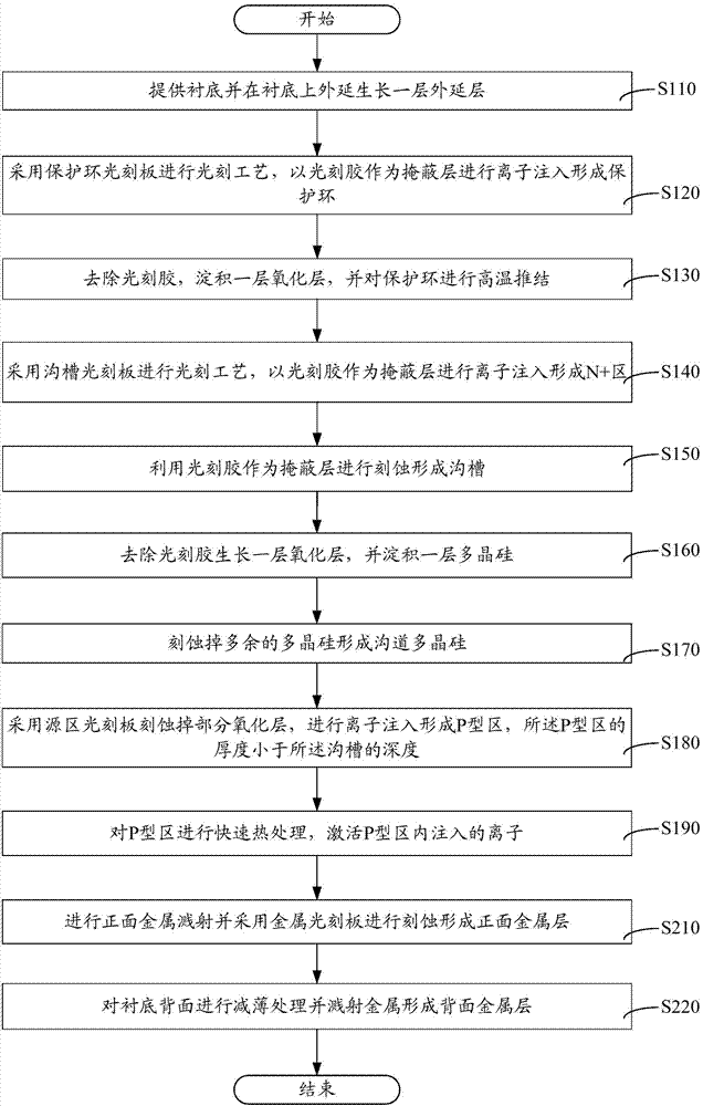
[0027] Please refer to image 3 , another embodiment provides a method for manufacturing a rectifier 100 . The manufacturing method of the rectifier 100 includes the following steps.

[0028] Step S110 , providing a substrate 111 and epitaxially growing an epitaxial layer 112 on the substrate 111 . Please refer to Figure 4, the substrate 111 used in the rectifier 100 is an N-type substrate 111 , the crystal orientation is , and the epitaxial layer 112 is an N-type epitaxial layer 112 . The thickness of the epitaxial layer 112 is 2-20 microns, and the resistivity of the epitaxial layer 112 is 0.5-5 Ω·cm. Here, the thickness and resistivity of the epitaxial layer 112 are designed according to the actual withstand voltage requirement. In addition, there is an oxide layer 115a above the epitaxial layer 112, and the oxide layer 115a can prevent loss of the epitaxial layer 112 during ion implantation.

[0029] In step S120 , a photolithography process is performed using a guar...


PUM


Abstract

The invention provides a rectifier and a manufacturing method thereof. The rectifier comprises a cellular region and a protection ring region. The cellular region comprises multiple rectifier diodes. Each rectifier diode comprises a substrate, an epitaxial layer arranged on the substrate, a P-type region arranged on the epitaxial layer, a groove penetrating through the P-type region, groove poly-crystalline silicon arranged in the groove, an oxide layer arranged between the groove wall of the groove and the groove poly-crystalline silicon, an N+ region arranged in the P-type region and positioned at the two sides of the groove, a front surface metal layer arranged on the P-type region, the N+ region and the groove poly-crystalline silicon, and a back surface metal layer arranged at the back surface of the substrate. The rectifier adopts a groove-type MOS structure so that parasitic JFET resistance is eliminated, and forward conduction voltage drop of the rectifier can be further reduced. Meanwhile, area of the chip is reduced and cost of the device is reduced. The manufacturing method of the rectifier adopts four photo-etching boards of a protection ring photo-etching board, a groove photo-etching board, a source region photo-etching board and a metal photo-etching board so that the manufacturing method of the rectifier has advantages of being simple in technology and low in manufacturing cost.

Description

technical field [0001] The invention relates to the field of semiconductor devices, in particular to a rectifier and a manufacturing method thereof. Background technique [0002] Traditional rectifiers mainly include PN junction diodes and Schottky diodes. The PN junction diode has a large forward voltage drop and a long reverse recovery time. However, the PN junction diode has better stability and can work at high voltage. Schottky diodes are semiconductor devices made of noble metals (such as gold, silver, titanium, etc.) in contact with semiconductors to form heterojunction barriers. It has absolute advantages at low voltage, such as its small forward voltage drop, short reverse recovery time, and has a wide range of applications in high-speed fields. However, the Schottky diode has the problems of large reverse leakage current and high manufacturing cost. [0003] In order to improve diode performance, Junction Barrier Controlled Schottky Rectifier (JBS, Junction Bar...

Claims


Application Information

Patent Timeline
Patent Type & Authority Applications(China)
IPC IPC(8): H01L27/08H01L29/861H01L29/06H01L21/822
Inventor 钟圣荣王根毅邓小社周东飞
Owner CSMC TECH FAB2 CO LTD
Why Eureka
Try Eureka