

Method for preparing nano-porous silicon from Cu nano-particles by two-step auxiliary etching
A nanoporous, assisted etching technology, applied in semiconductor/solid-state device manufacturing, electrical components, circuits, etc., can solve problems such as nanoporous silicon that is not specified, and achieve the effects of easy industrial production, easy operation, and low production cost.
- Summary
- Abstract
- Description
- Claims
- Application Information
AI Technical Summary
Problems solved by technology
Method used
Image

Examples
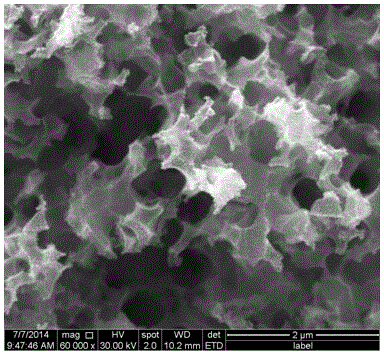
Embodiment 1
[0023] The method for preparing nanoporous silicon by two-step assisted etching of Cu nanoparticles, the specific steps are as follows:
[0024] Step 1. Silicon wafer pretreatment: ultrasonically clean the single crystal silicon wafer with a resistivity of 0.01Ω / cm, p-type, and a crystal orientation of (100) with acetone, toluene, ethanol, and deionized water for 20 minutes respectively;
[0025] Step 2, oxidation treatment on the surface of the silicon wafer: the silicon wafer pretreated in step 1 is immersed in an ultrasonic cleaning 2 SO 4 (15wt.%) and H 2 o 2 (10wt.%) soaked in a solution with a volume ratio of 3:1 for 10 minutes, an oxide layer can be formed on the surface of the silicon wafer;
[0026] Step 3, the preparation of deposition solution: make 10ml concentration be 0.1wt.%Cu(NO 3 ) 2 , 20ml of hydrofluoric acid with a concentration of 40wt.% and deionized water were prepared at a volume ratio of 10:20:70 to obtain 100ml of deposition solution;
[0027] S...
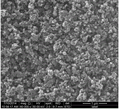
Embodiment 2
[0030] The method for preparing nanoporous silicon by two-step assisted etching of Cu nanoparticles, the specific steps are as follows:
[0031] Step 1. Silicon wafer pretreatment: ultrasonically clean the monocrystalline silicon wafer with a resistivity of 240Ω / cm, p-type, and crystal orientation (100) with acetone, toluene, ethanol, and deionized water for 20 minutes respectively;
[0032] Step 2, oxidation treatment on the surface of the silicon wafer: the silicon wafer pretreated in step 1 is immersed in an ultrasonic cleaning 2 SO 4 (15wt.%) and H 2 o 2 (10wt.%) soaked in a solution with a volume ratio of 3:1 for 10 minutes, an oxide layer can be formed on the surface of the silicon wafer;
[0033] Step 3, the preparation of deposition solution: make 10ml concentration be 0.1wt.%Cu(NO 3 ) 2 , 20ml of hydrofluoric acid with a concentration of 40wt.% and deionized water were prepared at a volume ratio of 10:20:70 to obtain 100ml of deposition solution;
[0034]Step 4,...
Embodiment 3
[0037] The method for preparing nanoporous silicon by two-step assisted etching of Cu nanoparticles, the specific steps are as follows:
[0038] Step 1. Silicon wafer pretreatment: ultrasonically clean the single crystal silicon wafer with a resistivity of 0.01Ω / cm, p-type, and a crystal orientation of (100) with acetone, toluene, ethanol, and deionized water for 20 minutes respectively;
[0039] Step 2, oxidation treatment on the surface of the silicon wafer: the silicon wafer pretreated in step 1 is immersed in an ultrasonic cleaning 2 SO 4 (15wt.%) and H 2 o 2 (10wt.%) soaked in a solution with a volume ratio of 3:1 for 10 minutes, an oxide layer can be formed on the surface of the silicon wafer;
[0040] Step 3, the preparation of deposition solution: make 10ml concentration be 0.1wt.%Cu(NO 3 ) 2 , 20ml of hydrofluoric acid with a concentration of 40wt.% and deionized water were prepared at a volume ratio of 10:20:70 to obtain 100ml of deposition solution;
[0041] S...
PUM
| Property | Measurement | Unit |
|---|---|---|
| electrical resistivity | aaaaa | aaaaa |
| electrical resistivity | aaaaa | aaaaa |
| electrical resistivity | aaaaa | aaaaa |
Abstract
Description
Claims
Application Information