Copper substrate-based nitride LED vertical chip and preparation method thereof

A technology of LED epitaxial wafers and copper substrates, applied in the direction of electrical components, circuits, semiconductor devices, etc., can solve the problems of complex process, low process yield, expensive equipment, etc., and achieve good current expansion, low thermal resistance, and high reliability sexual effect

Inactive Publication Date: 2015-04-29
江苏巨晶新材料科技有限公司
View PDF5 Cites 12 Cited by
  • Summary
  • Abstract
  • Description
  • Claims
  • Application Information

AI Technical Summary

Problems solved by technology

Vertical chips represented by thin-film chips usually use laser lift-off to separate the sapphire substrate and epitaxial layer, but this method is complex in process, expensive in equipment, and low in process yield

Method used


Image

  • Copper substrate-based nitride LED vertical chip and preparation method thereof
  • Copper substrate-based nitride LED vertical chip and preparation method thereof
  • Copper substrate-based nitride LED vertical chip and preparation method thereof

Examples


preparation example Construction

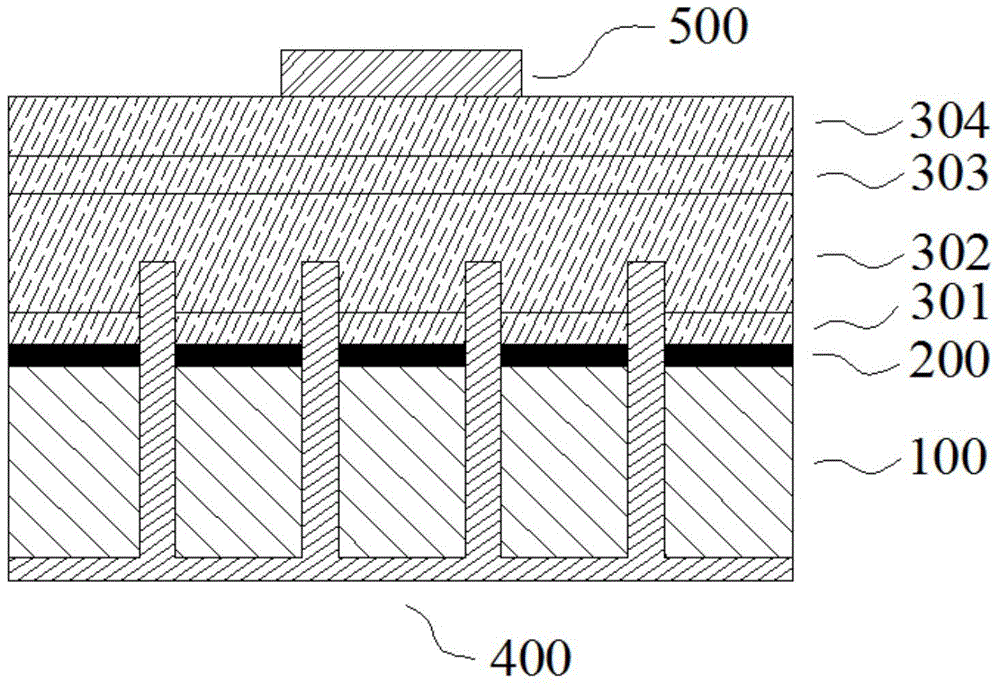
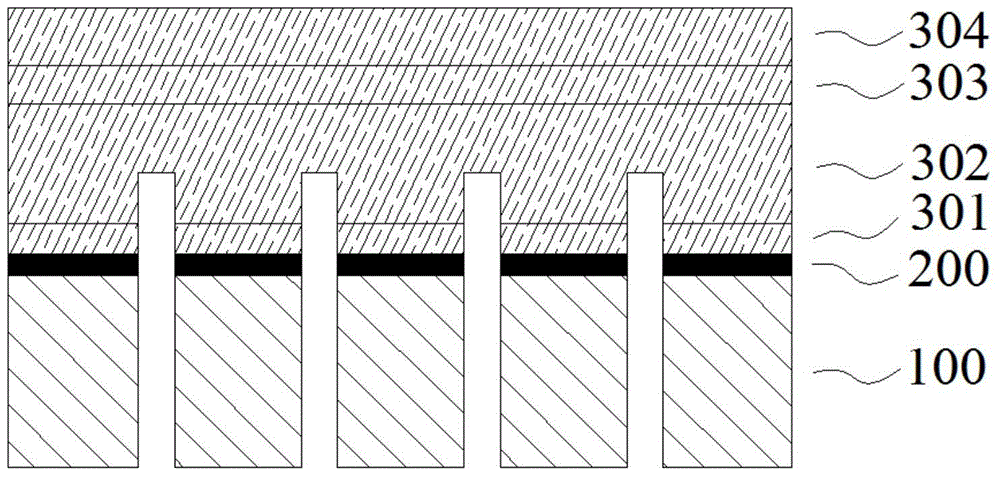
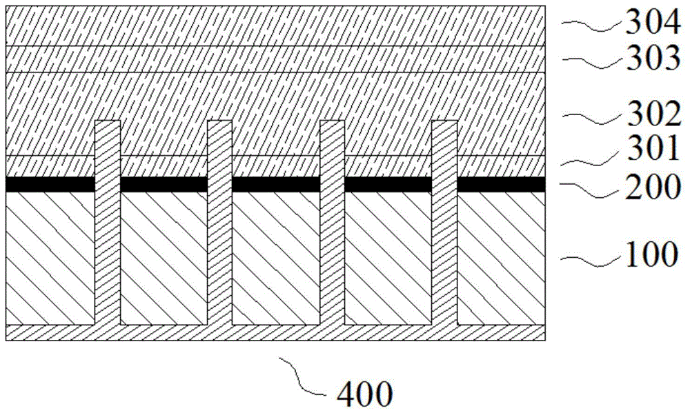
[0051] A method for preparing a nitride LED vertical chip based on a copper substrate, such as figure 2 , image 3 Shown, preparation method step is as follows:

[0052] 1) After preparing the nitride LED epitaxial wafer structure based on the copper substrate, use a perforation process to open holes from the back of the copper substrate to the buffer layer or n-type electron injection layer;

[0053] 2) Fabricate the metal channel structure to achieve ohmic contact with the n-type electron injection layer, and also realize the conduction between the n-type electron injection layer and the copper substrate. The metal channel structure and the copper substrate together form the n-type electrode;

[0054] 3) Fabricate a p-type electrode on top of the p-type hole injection layer.

[0055] The perforation process is a laser drilling process or a dry etching process. The light source of the laser drilling process is a pulse laser, and a single laser pulse width is less than 10 ...

Embodiment 1

[0076] Such as Figure 4 As shown, on top of a 2-inch, 80 μm thick copper substrate wafer 100, a single layer of graphene 201 is used as a two-dimensional derived film, and on the two-dimensional derived film is a nitride blue LED epitaxial layer. Wherein, the buffer layer 301 is made of 200nm n-type Al 0.1 Ga 0.9 N-layer composition; the structural parameters of the n-type electron injection layer 302 are as follows: a 2 μm thick n-type GaN layer, the doping element is Si, and the doping concentration is 1.0×10 19 ; The structural parameters of the active layer 303 are as follows: In 0.15 Ga 0.85 N / GaN multiple quantum well light-emitting layer, In 0.15 Ga 0.85 The single-layer thicknesses of N and GaN are 3nm and 10nm respectively, and the number of periods of the multiple quantum wells is 5; the structural parameters of the p-type hole injection layer 304 are as follows: it includes two sublayers, one is a 0.2 μm thick p-type GaN layer, The p-type doping element is Mg...

Embodiment 2

[0085] Such as Figure 6 As shown, on top of a 4-inch, 200 μm thick copper substrate wafer 100, a multi-layer hexagonal boron nitride (h-BN) 202 is used as a two-dimensional derived film, and a nitride blue LED is placed on the two-dimensional derived film epitaxial layer. Among them, the buffer layer 301 is made of 150nm n-type Al 0.3 Ga 0.7 N-layer structure; the structural parameters of the n-type electron injection layer 302 are as follows: a 2.5 μm thick n-type GaN layer, the doping element is Si, and the doping concentration is 1.5×10 19 ; The structural parameters of the active layer 303 are as follows: In 0.15 Ga 0.85 N / GaN multiple quantum well light-emitting layer, In 0.15 Ga 0.85 The single-layer thicknesses of N and GaN are 3nm and 10nm respectively, and the number of periods of the multiple quantum wells is 5; the structural parameters of the p-type hole injection layer 304 are as follows: it includes two sublayers, one is a 0.2 μm thick p-type GaN layer, T...


PUM

PropertyMeasurementUnit
thicknessaaaaaaaaaa
thicknessaaaaaaaaaa
thicknessaaaaaaaaaa

Abstract

The invention relates to a copper substrate-based nitride LED vertical chip and a preparation method thereof. The copper substrate-based nitride LED vertical chip comprises an n-type electrode, a two-dimensional derived film, a nitride epitaxial layer and a p-type electrode, wherein the two-dimensional derived film is attached onto the n-type electrode; the nitride epitaxial layer is attached onto the two-dimensional derived film; the p-type electrode is attached onto the nitride epitaxial layer. The preparation method for the copper substrate-based nitride LED vertical chip comprises the following steps: after a copper substrate-based nitride LED epitaxial wafer is prepared, piercing a hole from the back surface of a copper substrate to a buffer layer or an n-type electron injection layer by using a hole piercing process; manufacturing a metal channel structure for realizing the contact with the n-type electron injection layer, and simultaneously realizing the conduction between the n-type electron injection layer and the copper substrate; manufacturing the p-type electrode on the top of a p-type cavity injection layer. The nitride LED vertical chip disclosed by the invention has the characteristics of better current expanding, lower thermal resistance, higher reliability and the like, and is very suitable for the application directions of high current density driving and high optical power density output.

Description

technical field [0001] The invention relates to a nitride LED vertical chip based on a copper substrate and a preparation method thereof, belonging to the technical field of manufacturing LED optoelectronic devices. Background technique [0002] Al nitride x In y Ga 1-x-y N (0≤x, y≤1; x+y≤1; wurtzite crystal structure) light-emitting diode LEDs made of semiconductor materials are gradually being used in electronic display screens, landscape lighting, miner's lamps, Widely used in street lamps, liquid crystal display backlight, general lighting, optical disk information storage, biomedicine and other fields. The above-mentioned compound semiconductors can cover the entire spectral energy range from infrared, visible to ultraviolet light, and the emission wavelength of LED devices can be accurately customized by controlling the cationic composition of the nitride alloy. From the perspective of the scope of application fields and market capacity, the application of nitride ...

Claims


Application Information

Patent Timeline
Patent Type & Authority Applications(China)
IPC IPC(8): H01L33/14H01L33/40H01L33/36H01L33/00
CPCH01L33/0066H01L33/0075H01L33/32H01L33/36H01L33/40
Inventor 马亮胡兵刘素娟李金权裴晓将
Owner 江苏巨晶新材料科技有限公司
Why Eureka
Try Eureka