Graphene/silicon photodetector with passivated interface and preparation method thereof
A graphene and silicon photoelectric technology, applied in the field of photoelectric detection, can solve problems such as complex manufacturing processes, achieve low cost, increase photoelectric voltage, and facilitate promotion
- Summary
- Abstract
- Description
- Claims
- Application Information
AI Technical Summary
Problems solved by technology
Method used
Image

Examples
Embodiment 1
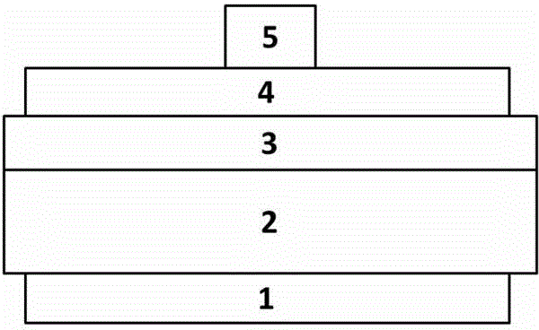
[0019] 1) Clean the p-type doped silicon substrate with a resistivity of about 1Ω·cm without damage on the surface, and dry it;
[0020] 2) A 0.2nm aluminum oxide layer is grown on one side of the silicon substrate using atomic layer deposition technology;
[0021] 3) Transfer single-layer graphene onto the alumina layer;
[0022] 4) Fabricate InGa alloy electrodes on the back of the silicon substrate;
[0023] 5) Coating silver paste on graphene and drying to obtain interface passivated graphene / silicon photodetector.
Embodiment 2
[0025] 1) Clean the n-type doped silicon substrate with a resistivity of about 1Ω·cm without damage on the surface, and dry it;
[0026] 2) A 1nm aluminum oxide layer is grown on one side of the silicon substrate using atomic layer deposition technology;
[0027] 3) Transfer 10 layers of graphene onto the alumina layer;
[0028] 4) Deposit gold electrodes on the back of the silicon substrate by thermal evaporation;
[0029] 5) A chromium-nickel composite electrode was deposited on graphene by magnetron sputtering to obtain an interface passivated graphene / silicon photodetector.
Embodiment 3
[0031] 1) Clean the n-type doped silicon substrate with a resistivity of about 10Ω·cm without damage on the surface, and dry it;
[0032] 2) A 10nm aluminum oxide layer is grown on one side of the silicon substrate using atomic layer deposition technology;
[0033] 3) Transfer 5 layers of graphene onto the alumina layer;
[0034] 4) Deposit titanium-palladium-silver composite electrodes on the back of the silicon substrate by electron beam evaporation;
[0035] 5) Deposit gold electrodes on graphene by magnetron sputtering to obtain interface passivated graphene / silicon photodetectors.
PUM
| Property | Measurement | Unit |
|---|---|---|
| thickness | aaaaa | aaaaa |
Abstract
Description
Claims
Application Information
 - R&D
- Intellectual Property
- Life Sciences
- Materials
- Tech Scout
- Unparalleled Data Quality
- Higher Quality Content
- 60% Fewer Hallucinations
Browse by: Latest US Patents, China's latest patents, Technical Efficacy Thesaurus, Application Domain, Technology Topic, Popular Technical Reports.
© 2025 PatSnap. All rights reserved.Legal|Privacy policy|Modern Slavery Act Transparency Statement|Sitemap|About US| Contact US: help@patsnap.com