Nano silicon boron slurry and method for preparing PERL solar battery by utilizing nano silicon boron slurry
A technology of nano-silicon-boron paste and solar cells, which is applied in the field of nano-materials to achieve the effect of low cost and simple process flow
- Summary
- Abstract
- Description
- Claims
- Application Information
AI Technical Summary
Problems solved by technology
Method used
Image
Examples
Embodiment 1
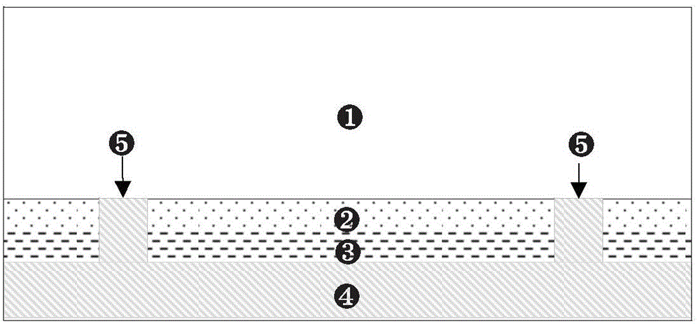
[0032] Embodiment 1: according to process route one, as image 3 Shown:
[0033] (1) Complete the following process according to the normal PERC battery preparation process: 1. Silicon wafer cleaning and flocking; 2. POCl 3 Diffusion to prepare emitter; 3. Cleaning and back polishing; 4. Deposition of Al on the back 2 o 3 Passivation film; 5. Double-sided deposition of SiNx film;
[0034] (2) Utilize screen printing equipment to locally print the nano-silicon-boron paste on the passivation film after the (1) process; the composition of the nano-silicon-boron paste is: 80 parts of sandalwood and 20 parts of nano-silicon powder, nano-silicon The average particle size is 50 nm, and the boron content is 5%. The printing pattern of the boron paste is a group of squares parallel to the edge of the silicon wafer and evenly arranged. The length of the side is 100um, and the distance between adjacent sides is 500um. The thickness of the boron paste is 2.5um.
[0035] (3) Dry the ...
Embodiment 2
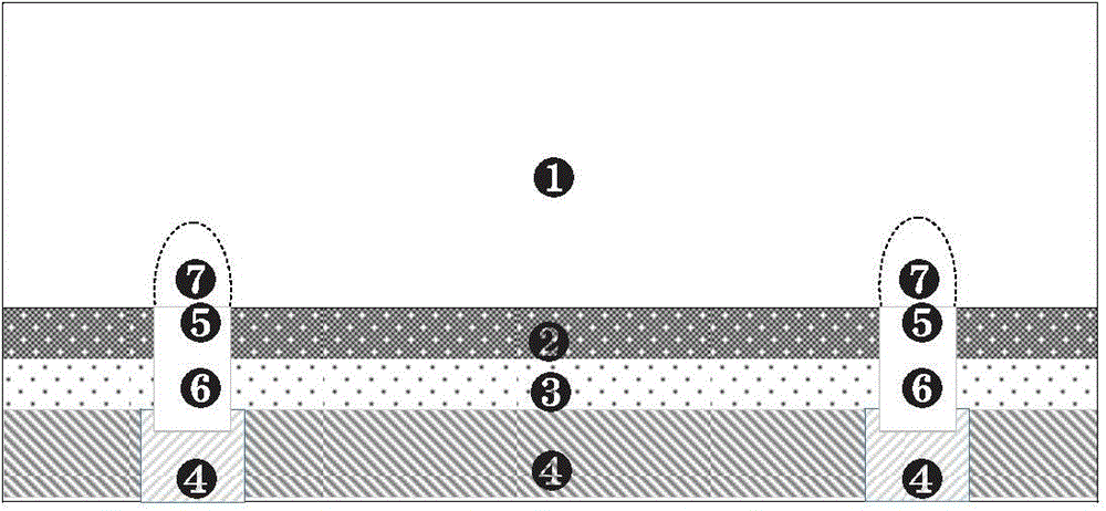
[0039] Embodiment 2: according to process route two, as Figure 4 Shown:
[0040] (1) According to the normal PERC cell preparation process, complete the front flocking and back polishing of the silicon wafer;
[0041] (2) Utilize screen printing equipment to locally print the nano-silicon boron paste on the back of the silicon wafer after the (1) process, that is, the polished surface; the composition of the nano-silicon boron paste is: 70 parts of sandalwood, 9 parts of terpineol, 1 part of ethyl cellulose, 20 parts of nano-silicon powder, the average particle diameter of nano-silicon is 70 nanometers, and the boron content is 8%. Printing boron paste is a group of square patterns parallel to the edge of the silicon wafer and evenly arranged, with a side length of 100um and a side distance of 500um.
[0042] (3) Dry the printed silicon wafer in an industrial infrared drying oven at a drying temperature of 170° C. and a drying time of 4 minutes.
[0043] (4) The silicon wa...
Embodiment 3
[0046] Embodiment 3: according to process route one, as image 3 Shown:
[0047] (1) Complete the following process according to the normal PERC battery preparation process: 1. Silicon wafer cleaning and flocking; 2. POCl 3 Diffusion to prepare emitter; 3. Cleaning and back polishing; 4. Deposition of Al on the back 2 o 3 Passivation film; 5. Double-sided deposition of SiNx film;
[0048] (2) Utilize screen printing equipment to locally print nano-silicon-boron paste on the passivation film after (1) process; the composition of nano-silicon-boron paste is: 60 parts of sandalwood, 19 parts of terpineol, 1 part of ethyl alcohol Base cellulose, 20 parts of nano-silicon powder, the average particle diameter of nano-silicon is 70 nanometers, and the boron content is 3%. The printing pattern of the boron paste is a group of squares parallel to the edge of the silicon wafer and evenly arranged, with a side length of 100um and a side distance of 500um. The thickness of boron past...
PUM
| Property | Measurement | Unit |
|---|---|---|
| particle diameter | aaaaa | aaaaa |
| thickness | aaaaa | aaaaa |
| thickness | aaaaa | aaaaa |
Abstract
Description
Claims
Application Information


