Organic electroluminescent device and production method thereof
An electroluminescent device and luminescence technology, which is applied in the direction of electric solid-state devices, semiconductor/solid-state device manufacturing, electrical components, etc., can solve the problems of desiccant loss of absorption capacity, device life reduction, and easy cracks, etc., to achieve a good level Coverage and large-area thickness uniformity, low impact, and strong adhesion effects
- Summary
- Abstract
- Description
- Claims
- Application Information
AI Technical Summary
Problems solved by technology
Method used
Image
Examples
Embodiment 1
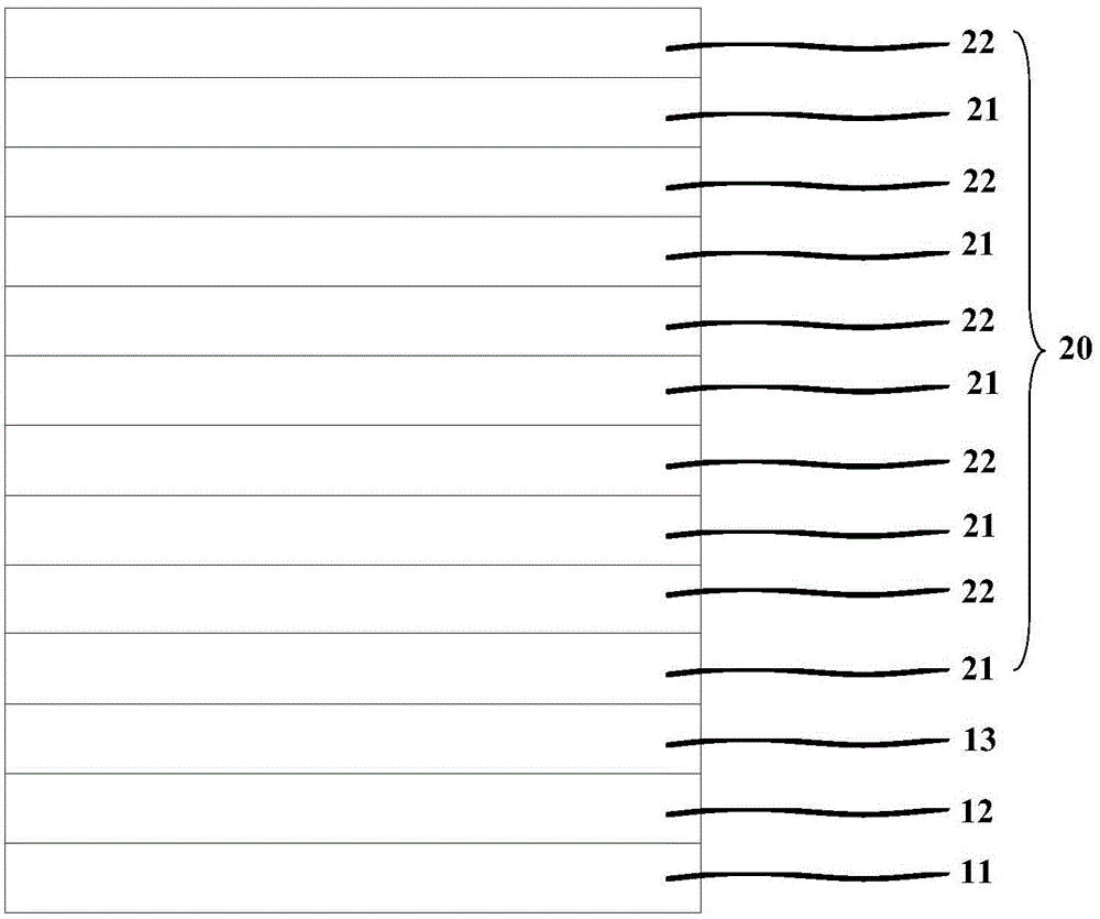
[0057] figure 1 is a schematic diagram of the organic electroluminescent device in embodiment 1; as figure 1 As shown, the organic electroluminescent device includes an ITO glass substrate (11), an organic light-emitting functional layer (12), a cathode (13) and an encapsulation layer (20); the encapsulation layer (20) includes five silicon oxynitride films An encapsulation unit composed of a layer (21) and an inorganic barrier layer (22).
[0058] A method for preparing an organic electroluminescent device, comprising the steps of:
[0059] (1) Pre-treatment of ITO glass substrate (11): First, clean the ITO glass with acetone, ethanol, deionized water, and ethanol in sequence, all of which are cleaned with an ultrasonic cleaner. dry, oven dry stand-by; then carry out surface activation treatment to the cleaned ITO glass, to increase the oxygen content of the conductive surface layer, improve the work function of the conductive layer surface; the thickness of the ITO glass s...
Embodiment 2
[0075] A method for preparing an organic electroluminescent device, comprising the steps of:
[0076] (1), (2), (3) are the same as embodiment 1;
[0077] (4) Preparation of encapsulation layer:
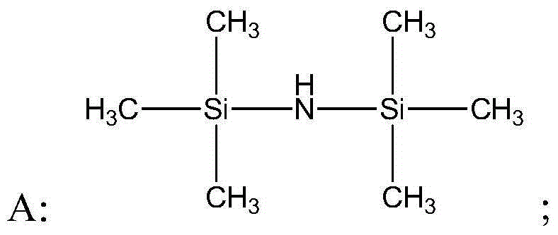
[0078] a) Preparation of silicon oxynitride film layer: a silicon oxynitride film layer was prepared on the cathode surface by plasma enhanced chemical vapor deposition (PECVD), the working pressure was 50Pa, the deposition temperature was 60°C, and the radio frequency power was 300W; The gas sources used in the process of depositing the silicon oxynitride layer are hexamethyldisilamine (HMDS), ammonia (NH 3 ) and oxygen (O 2 ), the loading gas is argon (Ar); the flow rate of hexamethyldisilamine (HMDS) is 14sccm, ammonia (NH 3 ) flow rate of 18sccm, oxygen (O 2 ) flow rate is 18 sccm, the flow rate of argon (Ar) is 80 sccm, and the thickness of the silicon oxynitride film layer is 190 nm;
[0079] b) Preparation of inorganic barrier layer: Atomic layer deposition (ALD) was used...
Embodiment 3
[0083] A method for preparing an organic electroluminescent device, comprising the steps of:
[0084] (1), (2), (3) are the same as embodiment 1;
[0085] (4) Preparation of encapsulation layer:
[0086] a) Preparation of silicon oxynitride film layer: a silicon oxynitride film layer was prepared on the cathode surface by plasma enhanced chemical vapor deposition (PECVD), the working pressure was 10Pa, the deposition temperature was 40°C, and the radio frequency power was 100W; The gas sources used in the process of depositing the silicon oxynitride layer are hexamethyldisilamine (HMDS), ammonia (NH 3 ) and oxygen (O 2 ), the loading gas is argon (Ar); the flow rate of hexamethyldisilamine (HMDS) is 12 sccm, ammonia (NH 3 ) flow rate is 15sccm, oxygen (O 2 ) flow rate is 16 sccm, the flow rate of argon (Ar) is 76 sccm, and the thickness of the silicon oxynitride film layer is 180 nm;
[0087] b) Preparation of inorganic barrier layer: Atomic layer deposition (ALD) is used...
PUM
| Property | Measurement | Unit |
|---|---|---|
| Thickness | aaaaa | aaaaa |
| Thickness | aaaaa | aaaaa |
| Thickness | aaaaa | aaaaa |
Abstract
Description
Claims
Application Information


