
Silicon-based laser device and method for manufacturing same

A laser and silicon-based technology, applied in phonon exciters, electrical components, circuits, etc., can solve the problems of insufficient intensity, insufficient luminous efficiency, and difficult preparation methods, and achieve simple structure, enhanced light wave intensity, and preparation The effect of simple process

Inactive Publication Date: 2015-06-10
HUAWEI TECH CO LTD +1
View PDF4 Cites 4 Cited by
  • Summary
  • Abstract
  • Description
  • Claims
  • Application Information

AI Technical Summary

Problems solved by technology

[0004] Silicon-based Raman lasers mainly use the stimulated Raman scattering effect in silicon and require high-power optical pumping, so their applications are limited; rare earth ion doped Si / SiO 2 Light-emitting devices are mainly doped with erbium Er 3+ Plasma is used to enhance light emission efficiency, but it is mainly prepared by electrical injection, and the preparation method is relatively difficult; quantum dots are introduced into silicon-based quantum dot lasers, and the wavelength of the emitted light can be adjusted by controlling the parameters of quantum dots, but its luminous efficiency It is still not high enough, the output power is small, and it cannot provide sufficient intensity of light at room temperature

Method used


Image

  • Silicon-based laser device and method for manufacturing same
  • Silicon-based laser device and method for manufacturing same
  • Silicon-based laser device and method for manufacturing same

Examples


preparation example Construction

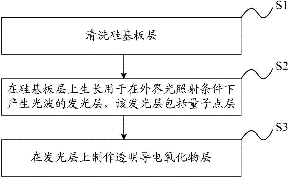
[0054] Correspondingly, as image 3 As shown, the present invention also provides a method for preparing a silicon-based laser, which can prepare any silicon-based laser provided by the embodiment of the present invention, and the preparation method includes:

[0055] S1, cleaning the silicon substrate layer;

[0056] S2. Growing a luminescent layer on the silicon substrate layer for generating light waves under the condition of external light irradiation, the luminescent layer includes a quantum dot layer;

[0057] S3. Fabricating a transparent conductive oxide layer on the light emitting layer.

[0058] The silicon-based laser manufacturing method provided by the embodiment of the present invention has simple process, low cost, and is easy to operate and realize.

[0059] Specifically, the fabrication of a transparent conductive oxide layer on the light-emitting layer in step S3 may specifically include:

[0060] Fabricate a discontinuous array made of transparent conduct...

Embodiment 1

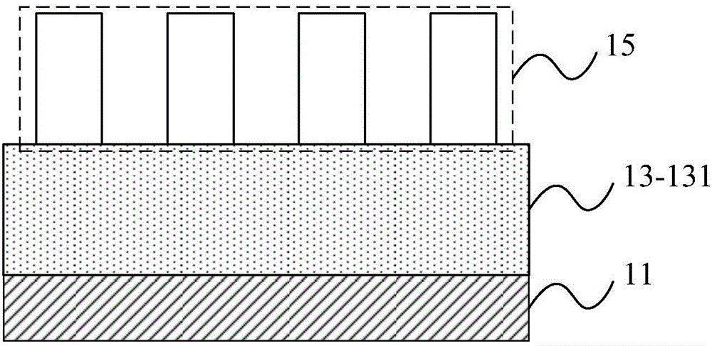
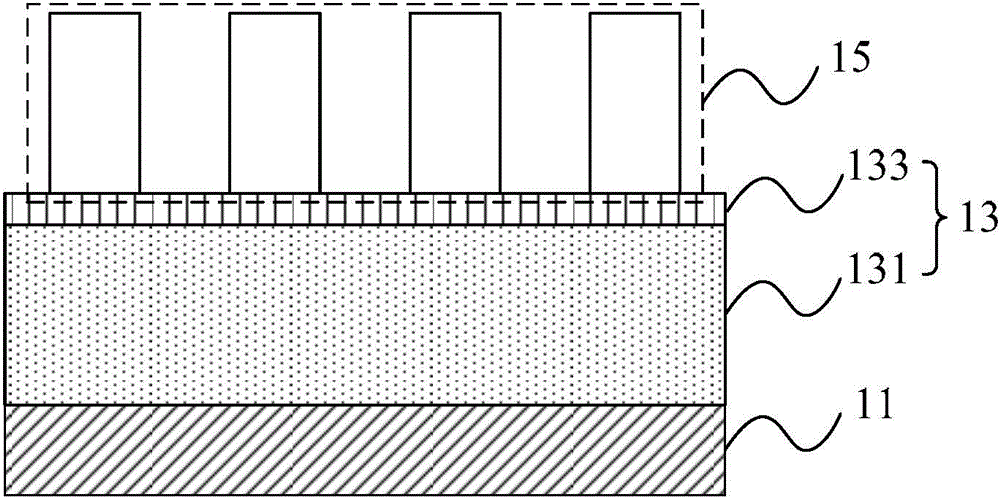
[0078] The silicon-based laser provided by the embodiment of the present invention includes a single-crystal silicon substrate, and a cylindrical periodic array of ten light-emitting layers and a layer of transparent conductive oxide are sequentially arranged on the single-crystal silicon substrate, wherein the light-emitting layer includes germanium quantum dots layer and a silicon protective layer positioned on the germanium quantum dot layer to prevent the quantum dot layer from being oxidized; specifically, the germanium quantum dots in the germanium quantum dot layer are all less than 50 nanometers in size, and the thickness of the protective layer is 15 nanometers , the cylinder periodic array parameters are 20 nm in height, 100 nm in diameter, and 400 nm in period.

[0079]When an external light source with a wavelength of 1550 nanometers is irradiated, the germanium quantum dots in the germanium quantum dot layer are excited to emit near-infrared light with a wavelength...

Embodiment 2

[0101] The difference from Embodiment 1 is that in Embodiment 1, the transparent conductive oxide is arranged as a periodic array of cylinders, while in the silicon-based laser provided by the embodiment of the present invention, the transparent conductive oxide is arranged as a periodic array of spheres, and the spheres are periodically The specific parameters of the array are: a diameter of 100 nanometers and a period of 400 nanometers.

[0102] Correspondingly, in the silicon-based laser preparation method of the embodiment of the present invention, the preparation steps of the transparent conductive oxide spherical periodic array are also different from the preparation steps of the transparent conductive oxide cylindrical periodic array provided in the first embodiment. The specific steps are:

[0103] Fabricating a periodic array of spherical transparent conductive oxides on the light-emitting layer is specifically: using a photoresist etching method to fabricate a period...


PUM

PropertyMeasurementUnit
Diameteraaaaaaaaaa
Diameteraaaaaaaaaa
Thicknessaaaaaaaaaa

Abstract

The invention provides a silicon-based laser device and a method for manufacturing the same, and relates to the technical field of semiconductors. The silicon-based laser device comprises a silicon substrate layer. A light emitting layer and a transparent conducting oxide layer are sequentially arranged on the silicon substrate layer, the light emitting layer comprises a quantum dot layer, and light waves can be generated by the quantum dot layer under external irradiation conditions; surface plasma resonance can be carried out on interfaces between the transparent conducting oxide layer and air under the external irradiation conditions; plasma resonance can be carried out on interfaces between the transparent conducting oxide layer and the light emitting layers under the external irradiation conditions. The silicon-based laser device and the method have the advantages that light with sufficiently high power can be outputted, light with sufficient intensity can be provided at normal temperatures, and the silicon-based laser device is simple in process and wide in application; the silicon-based laser device and the method are applicable to silicon-based integrated light sources in communication bands.

Description

technical field [0001] The invention relates to the technical field of semiconductors, in particular to a silicon-based laser and a preparation method thereof. Background technique [0002] With the development of silicon photonics technology, there is an urgent need for silicon-based light sources that can be integrated with optical waveguides, modulators or detectors on the same chip to meet the needs of optical communication and optical interconnection. However, since silicon is an indirect bandgap semiconductor, electrons cannot directly transition from the bottom of the conduction band to the top of the valence band to emit photons, but can only achieve indirect transitions by emitting or absorbing phonons. Since the probability of such indirect transitions is very small, so The light emission efficiency of silicon-based light sources is very low. [0003] Therefore, it is necessary to realize the silicon-based light source by adjusting the energy band and structure of...

Claims


Application Information

Patent Timeline
IPC IPC(8): H01S4/00
Inventor 叶辉夏亮杨迎春
Owner HUAWEI TECH CO LTD
Learn More