Method for improving thin-film semiconductor transistor electrical property

A thin-film semiconductor and electrical performance technology, applied in semiconductor/solid-state device manufacturing, circuits, electrical components, etc., can solve the problems of difficult industrial production, sacrificing device performance, electrical performance deterioration, etc., to achieve uniform thickness, high purity, Good coating or film-forming effect

Inactive Publication Date: 2015-06-17
SHANDONG UNIV
View PDF4 Cites 2 Cited by
  • Summary
  • Abstract
  • Description
  • Claims
  • Application Information

AI Technical Summary

Problems solved by technology

The results show that when the thickness of amorphous IGZO is reduced to 7nm or even lower, although the TFT still has a good device structure, its electrical performance has been seriously deteriorated, and the key parameter that characterizes the device performance, namely the mobility, has dropped to 0.3cm 2 / Vs
Although this method is expected to solve the cost problem in the device fabrication process, it is at the expense of device performance.
[0009] Literature [M.Mativenga,D.Geng,J.H.Chang,T.J.Tredwell,and J.Jang.Performance of 5-nm a-IGZO TFTs With Various Channel Lengths and an Etch Stopper Manufactured by Back UV Exposure.IEEE Electron Device Letters.2012 ,33:824] introduced the IGZO TFT with only 5nm with excellent characteristics. Their method is to connect the three cavities of the growth gate insulating layer, IGZO layer and packaging layer together, without breaking the vacuum. The preparation of the device is realized. Although this method also realizes the excellent performance of the ultra-thin IGZOTFT, the preparation equipment is very complicated and the preparation cost is high, which is difficult to realize in industrial production.

Method used


Image

  • Method for improving thin-film semiconductor transistor electrical property
  • Method for improving thin-film semiconductor transistor electrical property
  • Method for improving thin-film semiconductor transistor electrical property

Examples


Embodiment 1

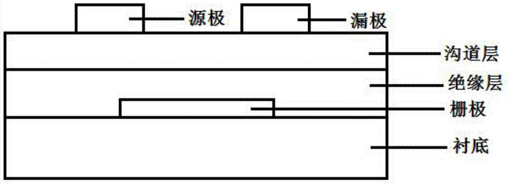
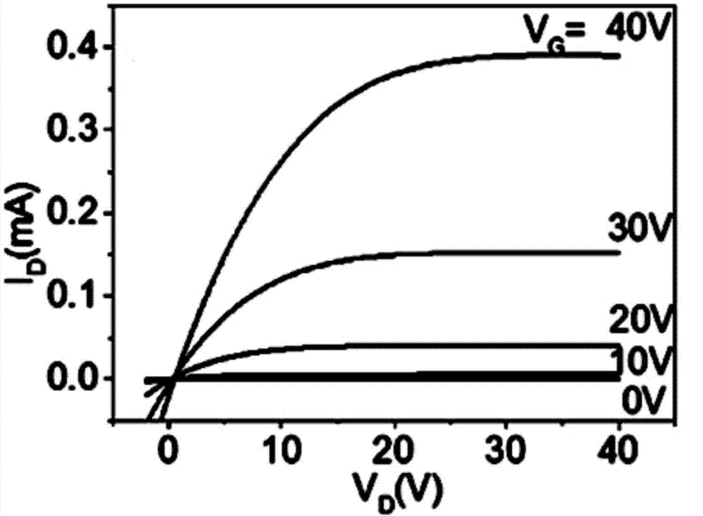
[0065] A method for improving the electrical performance of a thin film semiconductor transistor, specifically, covering the surface of the thin film semiconductor transistor with an organic layer.

[0066] The advantage of the design here is that an organic layer is covered on the surface of the thin film semiconductor transistor, on the one hand, the thin film semiconductor transistor is largely isolated from the outside air, and the H in the air is greatly reduced. 2 O, O 2 and (OH) - and other substances have a negative impact on the performance of thin film semiconductor transistors; on the other hand, it greatly reduces the defect states on the surface of thin film semiconductor transistors, because the surface defect states will bind the transport of carriers in the device, resulting in deterioration of the performance of thin film semiconductor transistors, Therefore, after covering an organic layer, the performance of the thin film semiconductor transistor is greatly...

Embodiment 2

[0069] According to the method for improving the electrical performance of the thin film semiconductor transistor described in Embodiment 1, the difference is that the organic layer is polyimide.

Embodiment 3

[0071] According to the method for improving the electrical performance of the thin film semiconductor transistor described in Embodiment 1, the difference is that the organic layer is a photoresist.


PUM


Abstract

The invention relates to a method for improving thin-film semiconductor transistor electrical property, in particular to that the surface of a thin-film semiconductor transistor is covered with an organic layer or an inorganic layer. Due to the fact that the surface of the thin-film semiconductor transistor is covered with the organic layer or the inorganic layer, on the one hand that the thin-film semiconductor transistor is separated from external air to a large extent, and the negative effects on the thin-film semiconductor transistor electrical property from substances such as H2O, O2, (OH)- and the like are greatly reduced; on the other hand that the defect mode of the surface of the thin-film semiconductor transistor is reduced to a large extent, since the surface defect mode can constrain the conveying of charge carriers in a device to lead to the deterioration of the thin-film semiconductor transistor property, the thin-film semiconductor transistor property can be greatly improved by covering the thin-film semiconductor transistor with the organic layer or the inorganic layer.

Description

technical field [0001] The invention relates to a method for improving the electrical performance of a thin film semiconductor transistor, belonging to the technical field of semiconductor devices. Background technique [0002] As a common metal semiconductor material, zinc oxide has a large energy band gap and exciton binding energy, high transparency, and excellent room temperature luminescence performance. It is widely used in liquid crystal displays, thin film transistors, light emitting diodes and other products in the semiconductor field. There are applications. [0003] Amorphous indium gallium zinc oxide (IGZO) is a ZnO material doped with In 2 o 3 and Ga 2 o 3 A new type of semiconductor material obtained later is widely used in the field of new generation thin film transistor technology, which is a kind of metal oxide Metal-Oxide panel technology. [0004] TFT (Thin Film Transistor) refers to a thin film field effect transistor, and a TFT liquid crystal screen...

Claims


Application Information

Patent Timeline
Patent Type & Authority Applications(China)
IPC IPC(8): H01L21/02
Inventor 张锡健张炳磊宋爱民
Owner SHANDONG UNIV
Why Eureka
Try Eureka