Preparation method and device for wafer grade white-light LED chip

An LED chip, wafer-level technology, applied in semiconductor/solid-state device manufacturing, electrical components, circuits, etc., can solve the problems of reducing packaging yield and packaging quality, high fluorescent glue content, difficult white light, etc., and achieves a simple production process. Reliable, simple and accurate operation, uniform brightness effect

Inactive Publication Date: 2015-07-01
LATTICE POWER (JIANGXI) CORP
View PDF5 Cites 8 Cited by
  • Summary
  • Abstract
  • Description
  • Claims
  • Application Information

AI Technical Summary

Problems solved by technology

Traditional packaging mainly has the following disadvantages: 1) After the blue-ray chip is installed on the packaging bracket, it is necessary to apply fluorescent glue to each chip, which leads to low work efficiency, large investment in packaging equipment, and high manufacturing costs; 2) The amount of fluorescent glue per chip The consistency is difficult to guarantee, so the packaging yield is low; 3) The fluorescent glue cannot be evenly distributed on the entire chip table, especially the microscopic amount of phosphor powder is difficult to match the microscopic blue light emission intensity, so the packaging quality is very low. Difficult to guarantee; 4) Apply fluorescent glue after chip bonding, which will easily lead to too much fluorescent glue on the gold ball part of the bonding wire, resulting in ball hanging phenomenon, greatly reducing packaging yield and packaging quality
For devices with the same side structure, its substrates are generally blue light-transmitting sapphire substrates and silicon carbide substrates. Even if the back of the chip is coated with an opaque reflective film, there will be light from five surfaces at the same time, so this structure It is most difficult to obtain white light with a uniform spot, and there will be an obvious yellow circle on the side of the chip

Method used


Image

  • Preparation method and device for wafer grade white-light LED chip
  • Preparation method and device for wafer grade white-light LED chip
  • Preparation method and device for wafer grade white-light LED chip

Examples


Embodiment 1

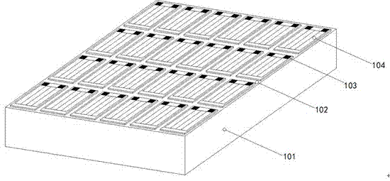
[0029] FIG. 1 is a specific step of preparing a wafer-level white LED chip according to the present invention. First, the epitaxially grown InGaAlN semiconductor light-emitting thin film on the silicon substrate is transferred to a conductive substrate to obtain an InGaAlN LED wafer with a vertical structure, such as Figure 1A shown. 101 in the figure is the conductive support substrate of the wafer; 102 is the dicing line gap between the chip arrays; 103 is the n-electrode pad of the chip; 104 is the blue light-emitting mesa of the InGaAlN thin film. The light emitting surface of the chip array is a nitrogen polar surface, the n electrode of the chip array is made on the nitrogen polar surface, the p electrode of the chip array is connected between the conductive substrate and the gallium nitride mesa by metal, the chip The p-electrode of the array contains metallic silver, and the light-emitting surface of the chip array is a roughened surface.

[0030] Figure 1B It is ...

Embodiment 2

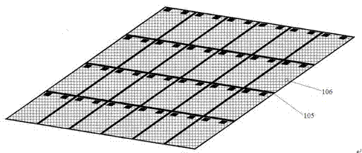
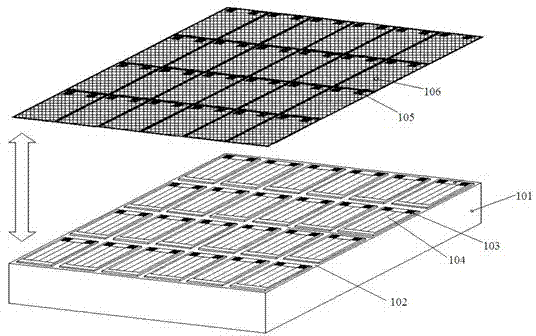
[0037] Fig. 2 is another embodiment of the present invention. The difference between this embodiment and Embodiment 1 is that the mesh mask body of this solution is only an independent whole formed by interconnecting mask patterns. like Figure 2A 201 is the conductive support substrate of the wafer; 202 is the InGaAlN LED blue light chip array; 203 is the mask pattern. Wherein the pad mask pattern on the mask pattern 203 is slightly smaller than the metal pad, this is for the white light chip to not leak blue light, and the dicing line mask pattern should also be compatible with the light-emitting table of the InGaAlN LED blue light chip array 202 A certain distance is also used to obtain uniform white light on the light-emitting table, and there is no area where blue light leaks. After finishing the alignment and lamination of the mask pattern 203 and the wafer, scrape the fluorescent glue 204 on it until the fluorescent glue 204 on the mask pattern 203 is scraped clean, a...

Embodiment 3

[0040] The mesh mask body in this embodiment is also made of a mask pattern, but this mask pattern is not made on the silk screen, nor is it separated from the wafer, it is directly made on the wafer, and is separated from the wafer The wafer becomes a whole mask pattern. It can be a mask pattern formed by a certain thickness of photoresist, or a metal mask pattern electroplated on a wafer. Before coating the leveling fluorescent glue, it is necessary to level the mask pattern on the wafer. Then apply fluorescent glue on its surface, scrape off the fluorescent glue on the mask pattern, then cure the fluorescent glue, and remove the mask pattern after the fluorescent glue is cured. If it is a mask pattern formed by photoresist, remove the photoresist with a sulfuric acid hydrogen peroxide mixture, or use an organic solvent to remove the photoresist, but the photoresist and its properties cannot be damaged while removing the photoresist. If it is a mask pattern formed of metal...


PUM


Abstract

The invention provides a preparation method and device for a wafer grade white-light LED chip. The method comprises the steps of forming a vertical structural aluminium gallium indium nitride LED wafer chip; adhering a mesh-shaped mask on the wafer chip, wherein the pattern of the mesh shaped mask covers only n electrode bonding pads and cutting channels in all chips on the wafer chip; coating fluorescent glue on the wafer chip on which the mesh shaped mask is adhered; scrapping and leveling the fluorescent glue through a scrapping knife; removing bubble; initially solidifying; separating the mesh shaped mask from the wafer chip; solidifying the fluorescent for the second time; scribing the wafer chip to obtain single chip. The white-light LED chip manufactured by the method has the advantages that the fluorescent powder cannot be damaged, the lighting brightness is uniform, the light outgoing surface is high, and the preparation process is simple and reliable.

Description

technical field [0001] The invention belongs to the field of manufacturing light emitting diodes. More specifically, the present invention relates to a method for preparing a vertical structure white LED chip by screen printing technology and a device for realizing the method. Background technique [0002] Light Emitting Diode (LED for short) is widely used in the lighting field, and the light in the lighting field is generally white light. The method to realize the white light emitting diode is usually to form a blue light chip first, and then add fluorescent light to the packaging material when packaging. Powder, the blue light emitted by the blue chip excites the phosphor in the packaging material to emit yellow light, green light, red light or a mixture of multiple colors, and the blue light and these excited lights are mixed together to form white light. Generally speaking, the preparation of blue light chips and white light packaging are relatively independent process...

Claims


Application Information

Patent Timeline
Patent Type & Authority Applications(China)
IPC IPC(8): H01L33/50H01L21/78
CPCH01L33/50H01L2933/0041
Inventor 熊传兵肖伟民刘声龙赵汉民
Owner LATTICE POWER (JIANGXI) CORP
Why Eureka
Try Eureka