A kind of microfluidic chip for sol method sers detection and its application method

A microfluidic chip and detection method technology, applied in the field of analytical chemistry, can solve the problems that cannot be used for Raman quantitative or semi-quantitative analysis, low repeatability of Raman detection of nanoparticle solution, etc., achieve low cost, expand application, time-consuming effect

Inactive Publication Date: 2017-11-17
XIAMEN UNIV
View PDF8 Cites 0 Cited by
  • Summary
  • Abstract
  • Description
  • Claims
  • Application Information

AI Technical Summary

Problems solved by technology

Therefore, to date, Raman detection of nanoparticle solutions has extremely low reproducibility and cannot be used for Raman quantitative or semi-quantitative analysis

Method used


Image

  • A kind of microfluidic chip for sol method sers detection and its application method
  • A kind of microfluidic chip for sol method sers detection and its application method
  • A kind of microfluidic chip for sol method sers detection and its application method

Examples


Embodiment 1

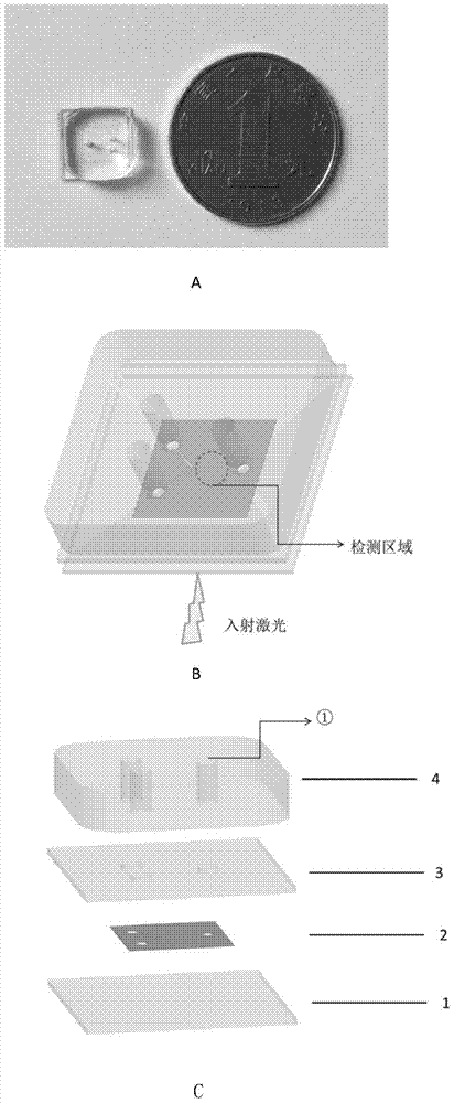
[0033] Prepare the chip for Raman detection, as attached figure 1 As shown, it consists of a backsheet, a film layer, a cover sheet, and a top layer.

[0034] The processing method of the chip: (1) choose a 1cm×1cm×300μm quartz plate as the bottom and cover, and use a laser engraving machine to process three round holes with a diameter of 0.5mm on the cover; (2) use the ultraviolet exposure method to prepare SU-8 photoresist mold, the mold is a raised Y-shaped channel with a height of 30 μm and a width of 50 μm; (3) Add the PDMS precursor dropwise on the SU-8 mold, cover with flat glass, pressurize, 115 Heat at ℃ for 15min to cure, and remove the cured PDMS film with adhesive tape; (3) activate the quartz plate and PDMS (polydimethylsiloxane) film under oxygen plasma, bond, remove the tape, and obtain a bonded (4) Align and bond the cover sheet and PDMS / quartz sheet after oxygen plasma activation, as the main body of the chip; (5) Make three holes with a diameter of 0.75mm in...

Embodiment 2

[0041] with 2x10 -5 M adenine and 6x10 -6 A mixed solution of sodium 4-mercaptophenylacetate (volume ratio 1:1) was used as the analyte. DSL test, the optimum acidity is 0.01M. In 100 μl Au@SiO 2 Add 100 μl of the solution to be tested and 50 μl of 0.01M sulfuric acid solution into the nanoparticle solution, mix well, then add 50 μl of equivalent NaOH solution, mix well, and flow into the chip from the hole of the chip at a speed of 300 μl / hr for detection .

[0042] As a control, in 100 μl Au@SiO 2 Add 100 μl 2x10 to the nanoparticle solution -5 M adenine and 6x10 -6 Mix solution of M4-sodium mercaptophenylacetate (volume ratio 1:1), and 50 μl 0.01M sulfuric acid solution, mix well, then add 50 μl equivalent NaOH solution, mix well, put it in a quartz cuvette for Raman detection.

[0043] Figure 6 The characteristic peak of 6 adenine Raman spectra in 50 measurements is 736.586cm -1 With 4-mercaptophenylacetic acid sodium characteristic peak 1076.26cm -1 Ratio curv...

Embodiment 3

[0046] Reagent 1: the concentration is 1x10 -4 M's 4-Mpy solution and a 10-fold concentrated solution of SHINERS particles;

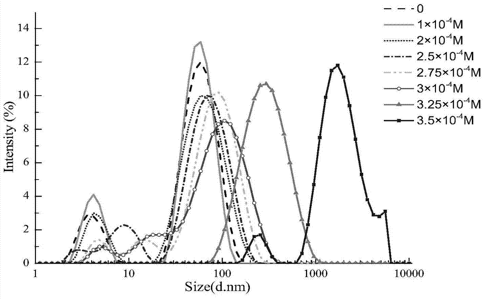
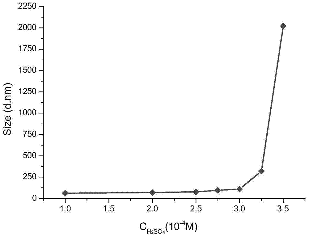
[0047] Reagent 2: Concentration of sulfuric acid solution: 1.0×10 -4 M, 2.0×10 -4 M, 2.5×10 -4 M, 2.75×10 -4 M, 3.0×10 -4 M, 3.25×10 -4 M, 3.5×10 -4 M.

[0048] Reagent 1 and reagent 2 flowed in from the first inlet and the second inlet of the chip respectively at a constant flow rate through a syringe, and observed the adherence condition under a microscope. The results show that when the acidity is less than a certain value, Raman peaks with a certain intensity can be generated, and there will be no agglomeration and no adhesion on the chip wall.


PUM

PropertyMeasurementUnit
heightaaaaaaaaaa
thicknessaaaaaaaaaa
heightaaaaaaaaaa

Abstract

The invention discloses a microfluidic chip for sol-based SERS detection and a method for using the same. The microfluidic chip includes a solution inlet and a solution outlet, and a detection area is arranged between the solution inlet and the solution outlet. , it is characterized in that: the detection area includes a sandwich structure, the upper and lower layers are quartz layers, the middle layer is a film layer, the film layer is provided with a hollow channel as the detection area, the hollow channel communicates with the solution inlet and the solution outlet, and the hollow channel The height is 10‑100 μm, the width is 40‑200 μm, the thickness of the upper layer is 300‑1000 μm, and the thickness of the lower layer is 100‑500 μm. Mix Au@SiO2 nanoparticles with a coating degree of 40-70% and the analyte, adjust the aggregate particle size of the system to 100 μm-300 μm with equivalent sulfuric acid and NaOH, and pass it into the chip for SERS detection. The invention can improve the repeatability of SERS detection.

Description

technical field [0001] The field of the present invention is the field of analytical chemistry, in particular to a highly reproducible Raman detection microfluidic chip and its application method. Background technique [0002] Raman scattering is a kind of vibration spectrum, but the intensity of ordinary Raman scattering spectrum is very weak, which limits its application in practical detection. Surface-Enhanced Raman scattering (SERS) can increase the Raman signal by 4-7 orders of magnitude, expanding the application of Raman spectroscopy in the field of scientific research. SERS uses special substrates (usually gold, silver, copper and other coin group metals) to enhance Raman signals. Common substrates include rough bulk substrates and nanoparticle solutions. Among them, the nanoparticle solution is widely used due to the advantages of simple preparation and convenient use. However, since the nanoparticle solution belongs to the colloidal solution, the agglomeration an...

Claims


Application Information

Patent Timeline
Patent Type & Authority Patents(China)
IPC IPC(8): G01N21/65B01L3/00
Inventor 江澄莹房晶焱周勇亮郭嘉
Owner XIAMEN UNIV
Why Eureka
Try Eureka