Radio frequency integrated circuit chip and its forming method

A technology of radio frequency integrated circuits and chips, which is applied in the direction of circuits, electrical components, and electric solid devices, and can solve problems such as harmonic distortion and adverse effects of signal linearity characteristics, and achieve the effect of improving transmission quality

Active Publication Date: 2018-06-01
SEMICON MFG INT (SHANGHAI) CORP
View PDF4 Cites 0 Cited by
  • Summary
  • Abstract
  • Description
  • Claims
  • Application Information

AI Technical Summary

Problems solved by technology

[0004] For the radio frequency integrated circuit chip (Chip) on the semiconductor substrate, when the radio frequency signal passes through active devices and passive devices (such as transmission lines or inductors) in the radio frequency integrated circuit, the radio frequency signal will be coupled with the semiconductor substrate , leading to harmonic distortion (Harmonic Distortion), which will have a great adverse effect on the linearity of the signal
[0005] To this end, a new radio frequency integrated circuit chip and its formation method are needed to prevent harmonic distortion caused by coupling between radio frequency signals and silicon-on-insulator substrates

Method used


Image

  • Radio frequency integrated circuit chip and its forming method
  • Radio frequency integrated circuit chip and its forming method
  • Radio frequency integrated circuit chip and its forming method

Examples


Embodiment Construction

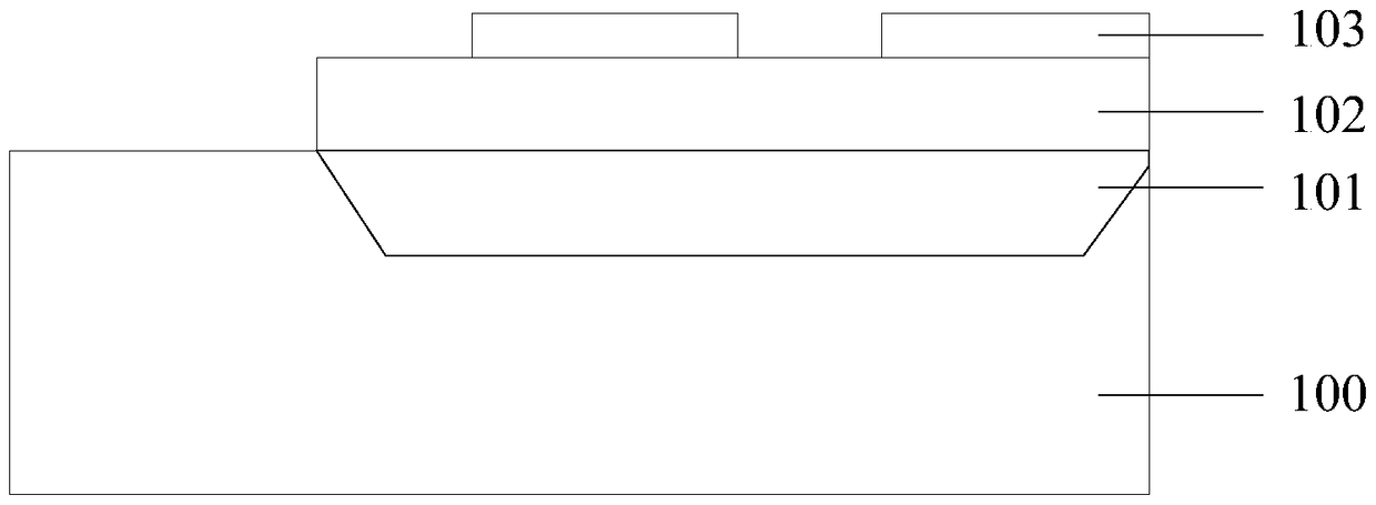
[0032] Such as figure 1 As shown, the existing radio frequency integrated circuit chip includes a high resistance semiconductor substrate 100 (High Resistance handle wafer), in which a shallow trench isolation structure 101 (STI) is usually fabricated, and a dielectric layer is also formed on the semiconductor substrate 100 102 (usually an interlayer dielectric layer or an intermetallic dielectric layer), a device 103 (usually an active device or a passive device) is formed on the dielectric layer 102 , wherein the passive device is usually located above the shallow trench isolation structure 101 .

[0033] Since the shallow trench isolation structure 101 inevitably carries fixed charges such as trap charges, which is equivalent to the gate oxide layer with a voltage applied in the transistor, it will provide high-resistance semiconductors that are located below it and are single-crystal structures. The substrate 100 generates an electric field, causing the high-resistance sem...


PUM


Abstract

A radio frequency integrated circuit chip and a method for forming the same, the radio frequency integrated circuit chip comprising: a semiconductor substrate having a shallow trench isolation structure in the semiconductor substrate; a filling layer penetrating through the shallow trench isolation structure and filling the Part of the semiconductor substrate is used to separate the semiconductor substrate from the shallow trench isolation structure; a dielectric layer is located on the semiconductor substrate, the shallow trench isolation structure and the filling layer; a radio frequency device , located on the dielectric layer. Since the semiconductor substrate and the shallow trench isolation structure are separated by a filling layer, it is possible to prevent the formation of a charge inversion layer or a charge accumulation layer between the semiconductor substrate and the shallow trench isolation structure, thereby preventing the semiconductor substrate from appearing similar to The conductive layer of the channel, so there will be no coupling capacitance between the radio frequency device and the semiconductor substrate, and when the radio frequency signal passes through the device, no harmonic distortion will occur, which improves the transmission quality of the radio frequency signal.

Description

technical field [0001] The invention relates to the field of semiconductor manufacturing, in particular to a radio frequency integrated circuit chip and a forming method thereof. Background technique [0002] Radio Frequency Integrated Circuit (RFIC), strictly speaking, refers to analog circuits that work in the frequency band above 0.8GHz, including microwave and millimeter wave circuits. [0003] Radio frequency integrated circuits mainly include filters, low noise amplifiers (LNA), voltage controlled oscillators (VCO), mixers, amplifiers / drivers, frequency synthesizers, power amplifiers (PA) and power management circuits. These radio frequency integrated circuits can be used to form a radio frequency transceiver, in which LNA, VCO, mixer, driver, etc. can be used to form the receiving front end of the signal receiving chain, that is, the receiver system; and the frequency synthesizer and power amplifier are used to form the transmitter. . The application of radio freque...

Claims


Application Information

Patent Timeline
Patent Type & Authority Patents(China)
IPC IPC(8): H01L21/762H01L23/66
Inventor 朱岩岩葛洪涛
Owner SEMICON MFG INT (SHANGHAI) CORP
Why Eureka
Try Eureka