

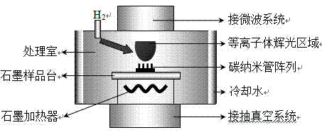
Method for improving field emission performance of carbon nano tube by microwave hydrogen plasma treatment
A technology of plasma and carbon nanotubes, which is applied in the field of preparation and application of nanomaterials, can solve the problems of shortening the service life of carbon nanotube-based field emission cathodes, poor field emission stability, and burning of effective field emission points, so as to improve field emission. The effect of emission performance
- Summary
- Abstract
- Description
- Claims
- Application Information
AI Technical Summary
Problems solved by technology
Method used
Image

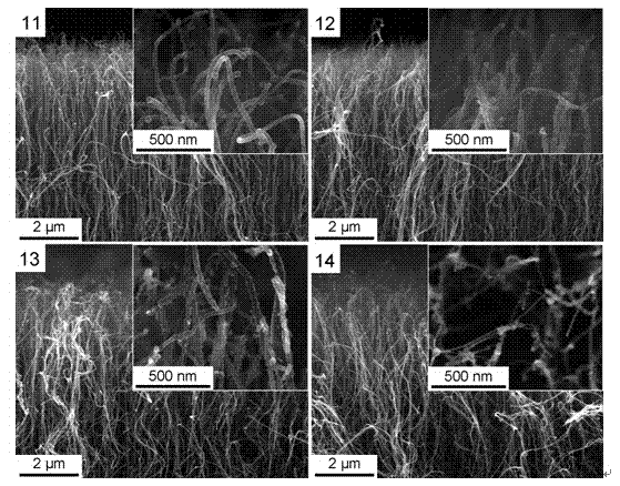
Examples
Embodiment 1
[0039] (1) Preparation of clean silicon wafer substrate:
[0040] First, cut the silicon wafer into small pieces of 2cm×2cm, clean them with ultrasonic (50W) in deionized water, acetone and absolute ethanol for 10 minutes, and then put the silicon wafer into hydrofluoric acid with a volume ratio of 4% for 5 minutes. Minutes for clean, contamination-free substrates free of silica overlays.
[0041] (2) Deposition of iron catalyst by magnetron sputtering:
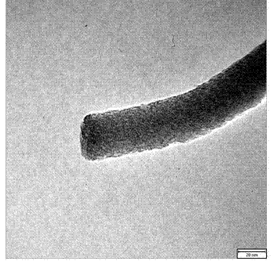
[0042] The deposition of the iron catalyst was carried out in a magnetron sputtering device (commercially available). Prior to this, the silicon single wafer was pretreated by bombardment with energetic iron ions in a metal vapor vacuum arc ion source (MEVVA source, commercially available). The iron ion energy was about 15keV, the beam current was 10 mA, and the processing time For 15 minutes, this treatment can effectively improve the bonding force between carbon nanotubes and silicon substrates; then place the silicon ...
Embodiment 2
[0052] (1) Preparation of clean silicon wafer substrate:
[0053] First, cut the silicon wafer into small pieces of 2cm×2cm, clean them with ultrasonic (50W) in deionized water, acetone and absolute ethanol for 10 minutes, and then put the silicon wafer into hydrofluoric acid with a volume ratio of 4% for 5 minutes. Minutes for clean, contamination-free substrates free of silica overlays.
[0054] (2) Deposition of iron catalyst by magnetron sputtering:
[0055] The deposition of the iron catalyst was carried out in a magnetron sputtering device (commercially available). Prior to this, the silicon single wafer was pretreated by bombardment with energetic iron ions in a metal vapor vacuum arc ion source (MEVVA source, commercially available). The iron ion energy was about 15keV, the beam current was 10 mA, and the processing time For 15 minutes, this treatment can effectively improve the bonding force between carbon nanotubes and silicon substrates; then place the silicon ...
Embodiment 3
[0065] (1) Preparation of clean silicon wafer substrate:
[0066] First, cut the silicon wafer into small pieces of 2cm×2cm, clean them with ultrasonic (50W) in deionized water, acetone and absolute ethanol for 10 minutes, and then put the silicon wafer into hydrofluoric acid with a volume ratio of 4% for 5 minutes. Minutes for clean, contamination-free substrates free of silica overlays.
[0067] (2) Deposition of iron catalyst by magnetron sputtering:
[0068] The deposition of the iron catalyst was carried out in a magnetron sputtering device (commercially available). Prior to this, the silicon single wafer was pretreated by bombardment with energetic iron ions in a metal vapor vacuum arc ion source (MEVVA source, commercially available). The iron ion energy was about 15keV, the beam current was 10 mA, and the processing time For 15 minutes, this treatment can effectively improve the bonding force between carbon nanotubes and silicon substrates; then place the silicon ...
PUM
| Property | Measurement | Unit |
|---|---|---|
| diameter | aaaaa | aaaaa |
| diameter | aaaaa | aaaaa |
| thickness | aaaaa | aaaaa |
Abstract
Description
Claims
Application Information