
A preparation method for optically controlled thin film transistors based on metal/organic shell core quantum dot-semiconductor quantum dot composite structure

A thin-film transistor and composite structure technology, which is applied in semiconductor/solid-state device manufacturing, semiconductor devices, electric solid-state devices, etc., can solve the problems of limited overall device performance, complicated preparation process, limited sensitivity, switching frequency and speed, and achieve device The effect of flexible and controllable performance, simple preparation process and novel preparation method

Active Publication Date: 2017-06-06
FUZHOU UNIV
View PDF6 Cites 0 Cited by
  • Summary
  • Abstract
  • Description
  • Claims
  • Application Information

AI Technical Summary

Problems solved by technology

This traditional thin film field effect transistor based on silicon microelectronics technology has problems such as high equipment requirements, complicated manufacturing process, high cost, limited overall performance of the device, limited sensitivity, switching frequency and speed, etc.
Moreover, with the gradual improvement of people's requirements for high-performance thin-film transistors, thin-film field-effect transistors based on microelectronic silicon technology have been difficult to meet the needs of today's information society for thin-film field-effect transistors with high sensitivity, high switching frequency and switching speed.

Method used


Image

  • A preparation method for optically controlled thin film transistors based on metal/organic shell core quantum dot-semiconductor quantum dot composite structure
  • A preparation method for optically controlled thin film transistors based on metal/organic shell core quantum dot-semiconductor quantum dot composite structure
  • A preparation method for optically controlled thin film transistors based on metal/organic shell core quantum dot-semiconductor quantum dot composite structure

Examples


Embodiment 1

[0032] (1) Weigh 0.0207g of cadmium oxide powder, 0.112g of 1-tetradecylphosphoric acid and 2.0g of tri-n-butylphosphine oxide into a 50ml three-necked flask, first evacuate with argon for 30min, and then under argon protection Heat to 240°C until the solute is completely dissolved to form a transparent solution, which is the cadmium precursor solution; then mix the cadmium precursor solution reactor and treat it under vacuum at 100°C for 0.5 hours, then adjust the reactor temperature to 250°C ;

[0033] (2) Weigh 0.0316g of selenium powder and 1.0g of tributylphosphine into another 50ml three-neck flask, and then heat to 100°C under the protection of argon until the solute is completely dissolved to form a transparent solution to obtain the selenium precursor solution;

[0034] (3) Rapidly inject the selenium precursor solution into the cadmium precursor solution, then lower the temperature of the mixed solution to 220 ° C, and keep it at this temperature for 1 min; then rem...

Embodiment 2

[0041] (1) Weigh 0.0812g of cadmium oxide powder, 0.336g of 1-tetradecylphosphoric acid and 1.5g of tri-n-butylphosphine oxide into a 50ml three-necked flask, first evacuate with argon for 80min, and then under argon protection Heat to 300°C until the solute is completely dissolved to form a transparent solution, which is the cadmium precursor solution; then mix the cadmium precursor solution reactor and treat it under vacuum at 120°C for 2 hours, then adjust the reactor temperature to 300°C;

[0042] (2) Weigh 0.084g of selenium powder and 3.0g of tributylphosphine into another 50ml three-necked flask, and then heat to 160°C under the protection of argon until the solute is completely dissolved to form a transparent solution to obtain the selenium precursor solution;

[0043] (3) Rapidly inject the selenium precursor solution into the cadmium precursor solution, then lower the temperature of the mixed solution to 250°C, and keep it at this temperature for 12 minutes; then rem...

Embodiment 3

[0050](1) Weigh 0.1028g of cadmium oxide powder, 0.448g of 1-tetradecylphosphoric acid and 1.0g of tri-n-butylphosphine oxide into a 50ml three-necked flask, first evacuate with argon for 120min, and then under argon protection Heat to 360°C until the solute is completely dissolved to form a transparent solution, which is the cadmium precursor solution; then mix the cadmium precursor solution reactor and treat it under vacuum at 130°C for 3 hours, then adjust the reactor temperature to 330°C;

[0051] (2) Weigh 0.1264g of selenium powder and 4.0g of tributylphosphine into another 50ml three-necked flask, and then heat to 220°C under the protection of argon until the solute is completely dissolved to form a transparent solution to obtain the selenium precursor solution;

[0052] (3) Rapidly inject the selenium precursor solution into the cadmium precursor solution, then lower the temperature of the mixed solution to 270°C, and keep it at this temperature for 20 minutes; then re...


PUM


Abstract

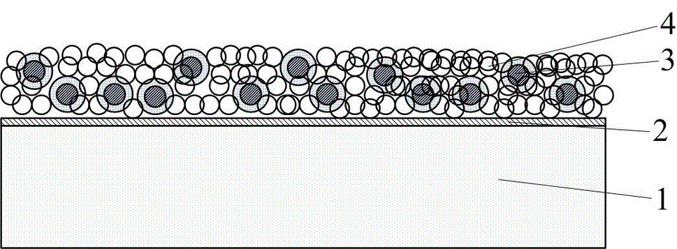
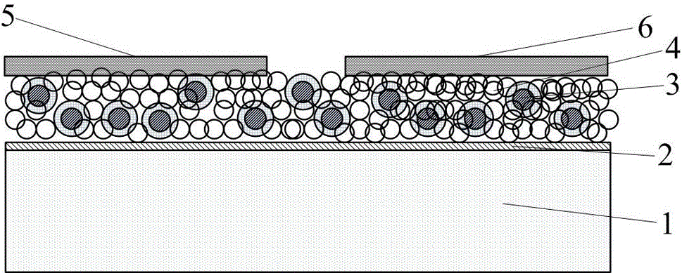
The invention relates to a method for preparing an optically controlled thin film transistor based on a metal / organic shell core quantum dot-semiconductor quantum dot composite structure, using spin-coating film forming technology to prepare a metal / organic shell core quantum dot-semiconductor quantum dot on a silicon / silicon dioxide substrate. Organic shell core quantum dot-semiconductor quantum dot composite film layer, and then cover the evaporation process technology metal / organic shell core quantum dot-semiconductor quantum dot composite conductive channel layer through a patterned mask to form Cr / Au composite metal electrodes , lead to the corresponding source and drain, and then realize the effective packaging and protection of the quantum dot channel by spin-coating organic matter, so as to prepare a new type of optical control film based on metal / organic shell core quantum dot-semiconductor quantum dot composite structure transistor. The preparation method of the present invention is novel, the production cost is low and the process is simple, and at the same time, the effect of metal quantum dot plasmons on light field enhancement regulation and the quantum size effect of the composite quantum dot film can be fully utilized, thereby effectively improving the optical control gate transistor. sensitivity.

Description

technical field [0001] The invention belongs to the field of semiconductor nanomaterials and devices, and in particular relates to a method for preparing an optically controlled thin film transistor based on a metal / organic shell core quantum dot-semiconductor quantum dot composite structure. Background technique [0002] With the development of science and technology and the progress of society, people are increasingly dependent on information storage, transmission and processing. As the main carrier and material basis of information storage, transmission and processing, semiconductor devices and process technology have become a hot spot for many scientists to study. Thin film transistors, as a very important semiconductor device, play a vital role in the fields of information storage, transmission and processing. However, as of now, the existing large-scale use of thin-film transistors is a semiconductor device based on silicon technology for microelectronics. This tradi...

Claims


Application Information

Patent Timeline
Patent Type & Authority Patents(China)
IPC IPC(8): H01L51/40H01L51/30
CPCH10K71/12H10K85/00H10K10/00H10K10/488H10K10/88
Inventor 杨尊先郭太良胡海龙周雄图吕军杨洋
Owner FUZHOU UNIV
Learn More