
Method for preparing thin-film transistor based on scandia high-k dielectric layer

A technology of thin-film transistors and dielectric layers, applied in semiconductor/solid-state device manufacturing, circuits, electrical components, etc., to achieve the effects of reliable principles, reduced production costs, and cheap processes

Inactive Publication Date: 2015-09-23
QINGDAO UNIV
View PDF7 Cites 7 Cited by
  • Summary
  • Abstract
  • Description
  • Claims
  • Application Information

AI Technical Summary

Problems solved by technology

Through the review of relevant patents and literature, there are few reports on the preparation of TFT channel layers by the "water-based sol" method. 2 o 3 All-aqueous TFT devices with high-k dielectric layers are even more unexplored

Method used


Image

  • Method for preparing thin-film transistor based on scandia high-k dielectric layer
  • Method for preparing thin-film transistor based on scandia high-k dielectric layer
  • Method for preparing thin-film transistor based on scandia high-k dielectric layer

Examples


Embodiment

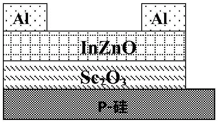
[0022] The scandium nitrate, zinc nitrate and indium nitrate powders involved in this embodiment are all purchased from Aldrich Company, and the purity is greater than 98%; its bottom gate structure is based on ultra-thin scandium oxide (Sc 2 o 3 ) is a high-k dielectric layer and the preparation process of an all-aqueous thin film transistor with an indium zinc oxide (IZO) film as a channel layer is:

[0023] (1) Prepare ultra-thin Sc by spin-coating with aqueous sol method 2 o 3 High-k dielectric films:

[0024] Step 1: Select commercially purchased single-sided polished low-resistance silicon as the substrate (resistance value less than 0.0015 Ω·cm) and the gate electrode, and clean the low-resistance silicon substrate with hydrofluoric acid, acetone, and alcohol ultrasonically for 10 times each. Minutes, and then rinsed repeatedly with deionized water, then blow dry with high-purity nitrogen;

[0025] Step 2: Weigh 10mL of deionized water, dissolve scandium nitrate in ...


PUM

PropertyMeasurementUnit
thicknessaaaaaaaaaa
electrical resistivityaaaaaaaaaa
thicknessaaaaaaaaaa

Abstract

The invention belongs to the technical field of semiconductor thin film transistor preparation technology and relates to a method for preparing a thin-film transistor based on a scandia high-k dielectric layer. According to the method, firstly, scandium nitrate is dissolved in de-ionized water and the obtained solution is stirred to form a precursor solution. The precursor solution is applied onto the cleaned surface of a low-resistance silicon substrate through the spin-coating process and the spin-coating thickness is 5-10 nm. After that, a thin film generated through the spin-coating process is baked and annealed to obtain a Sc2O3 film sample. Then, the zinc nitrate and the indium nitrate are respectively dissolved in de-ionized water and stirred to form an IZO aqueous solution. The IZO aqueous solution is applied onto the surface of the Sc2O3 film sample through the spin-coating process. After the spin-coating process, the film sample is cured and annealed at a low temperature to obtain an IZO channel layer. Finally, a metal source and a drain electrode are prepared on the IZO channel layer by means of a stainless steel mask through the vacuum thermal-evaporation process, so that a thin-film transistor can be obtained. According to the overall technical scheme of the invention, the method has the advantages of low cost, simple process, reliable principle, good product performance, environment-friendly preparation and broad application prospect. By utilizing the method, the large-area preparation of high-performance thin-film transistors is realized.

Description

Technical field: [0001] The invention belongs to the technical field of semiconductor thin film transistor preparation, and relates to a method for preparing a thin film transistor based on a green and environmentally friendly water-based sol. 2 o 3 ) is a high-k dielectric layer, and water-based indium zinc oxide (InZnO) is used as a semiconductor channel layer to prepare a transistor with a thin film structure. Background technique: [0002] Currently, thin film transistors (Thin Film Transistor, TFT) play an important role in active matrix liquid crystal display devices (Active Matrix Liquid Crystal Display, AMLCD). From low-temperature amorphous silicon TFTs to high-temperature polysilicon TFTs, the technology is becoming more and more mature, and the application objects have also developed from only driving LCD (Liquid Crystal Display) to driving both LCD and OLED (Organic Light Emitting Display) and electronic paper. TFT has become the core component of the flat pane...

Claims


Application Information

Patent Timeline
Patent Type & Authority Applications(China)
IPC IPC(8): H01L21/336H01L21/28
CPCH01L29/66742H01L21/28158
Inventor 单福凯刘奥刘国侠
Owner QINGDAO UNIV
Learn More