
Method for preparing GaMnN diluted magnetic semiconductor thin film material

A technology of dilute magnetic semiconductor and thin film materials, applied in the application of magnetic film to substrate, metal material coating process, gaseous chemical plating, etc., can solve the problems of complex tail gas treatment process, expensive raw materials, high maintenance cost, etc. Achieve the effects of short production cycle, good crystal quality and low preparation cost

Inactive Publication Date: 2015-11-04
QILU UNIV OF TECH
View PDF1 Cites 1 Cited by
  • Summary
  • Abstract
  • Description
  • Claims
  • Application Information

AI Technical Summary

Problems solved by technology

In addition, the above method also has disadvantages such as high equipment maintenance cost, expensive raw materials, long production cycle and complicated tail gas treatment process.

Method used


Image

  • Method for preparing GaMnN diluted magnetic semiconductor thin film material
  • Method for preparing GaMnN diluted magnetic semiconductor thin film material
  • Method for preparing GaMnN diluted magnetic semiconductor thin film material

Examples


Embodiment Construction

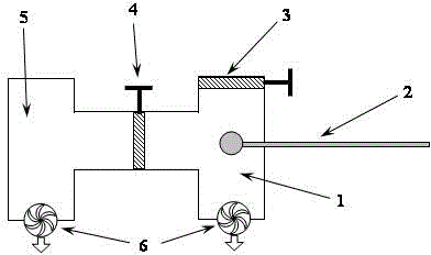
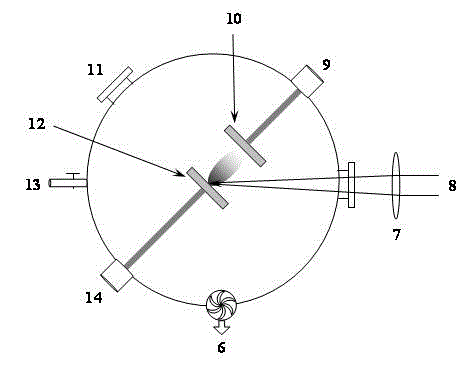
[0020] Please also see figure 1 with figure 2 , the technical features of the present invention will be further described below in conjunction with specific growth processes.

[0021] (1) Before preparing the GaMnN dilute magnetic semiconductor thin film material, the substrate was ultrasonically cleaned twice with acetone, each time for 10 minutes, after each cleaning, it was rinsed with deionized water for about 2 minutes, and then ultrasonically cleaned with ethanol for 10 minutes , and finally rinsed with deionized water and dried for later use.

[0022] (2) Put the GaN ceramic target on the transfer rod 2 through the valve 3 of the sampling chamber 1 . Turn on the mechanical pump of the vacuum system 6, and when the pressure in the growth chamber 5 reaches below 10 Pa, turn on the molecular pump of the vacuum system 6, pump for about 4 hours, and the background vacuum of the system can reach 5×10 -5 Below Pa. Then, the GaN ceramic target is put into a target positio...


PUM


Abstract

A diluted magnetic semiconductor thin film material appears many novel physical properties, and the novel physical properties provide a broader space for development of novel spin-based devices, so that the diluted magnetic semiconductor thin film material has broad application prospects in the fields of magnetic inductors, high-density non-volatile memories, optical isolators, semiconductor laser devices, spin quantum computers and the like, and has become one of research hot spots in the field of the materials. Traditional methods for preparing thin film materials comprise a molecular beam epitaxy method, a metal organic matter chemical vapor deposition method and the like, and the methods are balanced growth methods and have the shortcomings of low doping efficiency, high equipment maintenance cost, expensive price of raw materials, long production period, complex tail gas treatment process and the like. The invention belongs to the technical field of semiconductors and provides a method for preparing a GaMnN diluted magnetic semiconductor thin film material, and the method has the advantages of high doping efficiency, low preparation cost, short production period, simple tail gas treatment and the like, and can greatly improve the production efficiency and economic benefits.

Description

technical field [0001] The invention belongs to the field of semiconductor technology, in particular to a method for preparing GaMnN dilute magnetic semiconductor thin film material, especially a method of laser molecular beam epitaxy (LMBE) on sapphire (Al 2 o 3 ) on the substrate, and then prepare GaMnN dilute magnetic semiconductor thin film material by in-situ annealing method. Background technique [0002] Diluted Magnetic Semiconductor (DMS) refers to the fact that some cations in compound semiconductors are replaced by magnetic transition metals (such as Fe, Co, Ni, Mn, etc.) or rare earth metals (such as Sm, Eu, Gd, Tb, etc. ) A new type of semiconductor material formed by ion substitution, because the doped magnetic ion concentration is not high, so the magnetism is relatively weak, so it is called dilute magnetic semiconductor. Diluted magnetic semiconductor materials have both the properties of semiconductor materials and magnetic materials. In this type of mate...

Claims


Application Information

Patent Timeline
IPC IPC(8): C23C16/48C23C16/34C23C16/56H01F41/22
Inventor 高兴国
Owner QILU UNIV OF TECH
Learn More