Absorber of ultra wide band of visible and near-infrared band and preparation method thereof

An absorber and ultra-broadband technology, which is applied in the fields of imaging, space detection, stray light elimination, photothermal conversion and electromagnetic absorption, can solve the problems of low absorption rate and complicated preparation process, and achieve shortened production cycle, good absorption performance, Good incidence angle insensitivity effect

Active Publication Date: 2015-11-04
上海高能煜镀科技有限公司
View PDF6 Cites 22 Cited by
  • Summary
  • Abstract
  • Description
  • Claims
  • Application Information

AI Technical Summary

Problems solved by technology

The absorptivity of the coating is lower than

Method used


Image

  • Absorber of ultra wide band of visible and near-infrared band and preparation method thereof
  • Absorber of ultra wide band of visible and near-infrared band and preparation method thereof
  • Absorber of ultra wide band of visible and near-infrared band and preparation method thereof

Examples


preparation example Construction

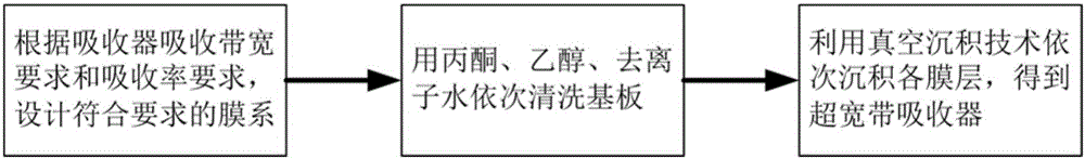
[0035] A preparation method of an ultra-broadband absorber in the visible-near-infrared band, comprising the following steps, such as figure 2 Shown:

[0036] 1) According to the required absorber bandwidth requirements and absorption rate requirements, by optimizing the thickness of each layer of film, design a film system that meets the requirements;

[0037] 2) put the substrate into the acetone solution for 8 minutes, then clean the substrate with ethanol; then put the substrate (substrate) into the ethanol solution for 8 minutes, then clean the substrate with deionized water; finally clean the substrate Put it in deionized water for 8 minutes, and then wash the substrate again with deionized water;

[0038] 3) Vacuum coating technology is used to deposit each film layer in sequence to obtain an ultra-broadband absorber in the visible-near infrared band;

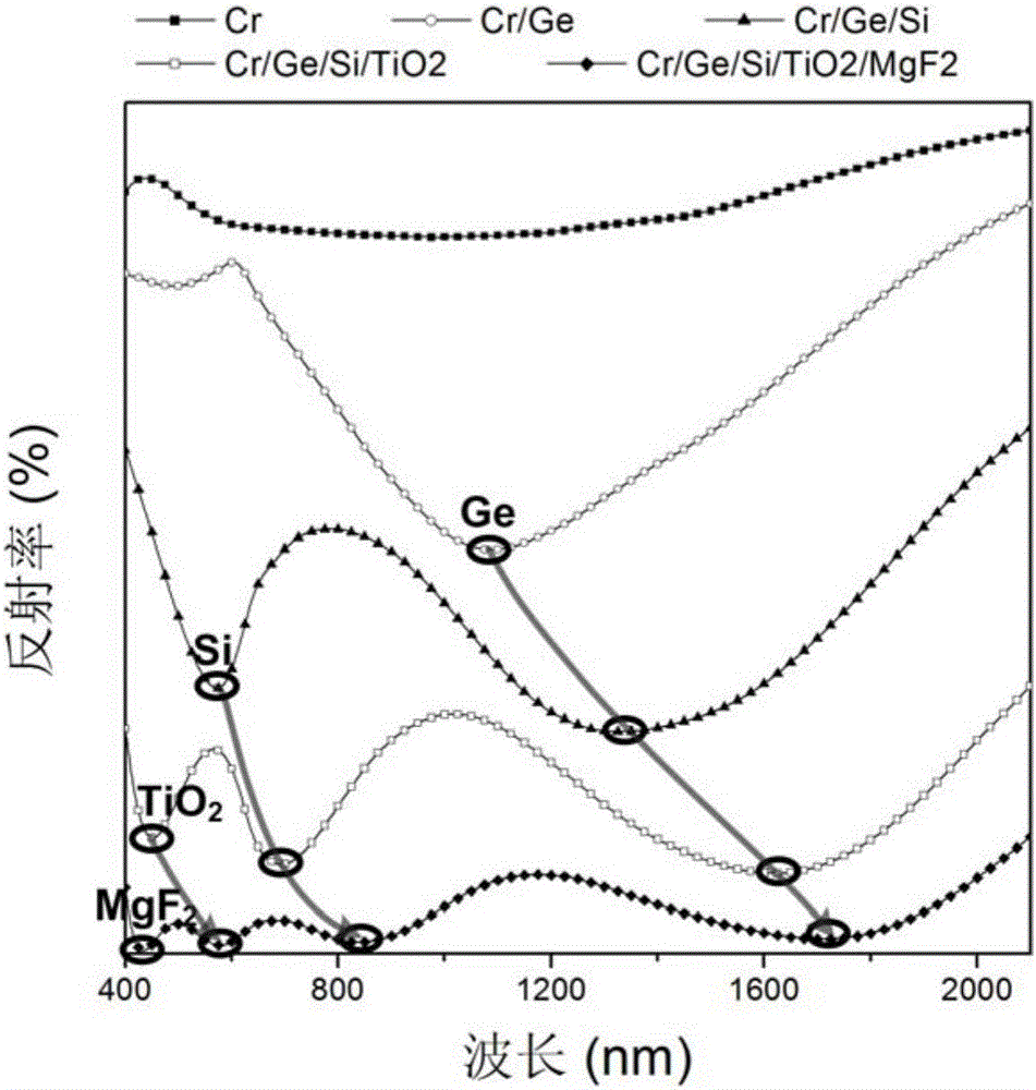
[0039] The ultra-broadband absorption of the ultra-broadband absorber in the visible-near-infrared band of the pres...

Embodiment 1

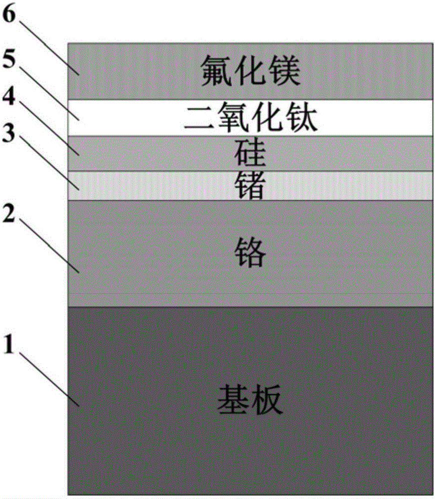
[0041] Embodiment 1: Visible-near-infrared band ultra-broadband absorber, the expected absorption bandwidth is 400nm-1200nm, and the average absorption rate is more than 98%. The absorption spectrum of the absorber sample prepared by the present invention is as follows: Figure 4 As shown in (a), the average absorption rate is above 98.75%. The corresponding base material is a silicon wafer, and the corresponding film materials are sequentially chromium, germanium, silicon, titanium dioxide, and magnesium fluoride. The corresponding film layers of each film layer The thicknesses are 200nm (chromium), 18nm (germanium), 19nm (silicon), 35nm (titanium dioxide), and 80nm (magnesium fluoride).

Embodiment 2

[0042] Embodiment 2: Visible-near-infrared band ultra-broadband absorber, the expected absorption bandwidth is 400nm-2000nm, and the absorption rate of each wavelength is more than 90%. The absorption spectrum of the absorber sample prepared by the present invention is as follows Figure 4 As shown in (b), the average absorption rate is above 97.75%. The corresponding base material is a silicon wafer, and the corresponding film layer materials are sequentially chromium, germanium, silicon, titanium dioxide, and magnesium fluoride. The film corresponding to each film layer The layer thicknesses are 200nm (chromium), 33nm (germanium), 32nm (silicon), 56nm (titanium dioxide), 118nm (magnesium fluoride), respectively.


PUM

PropertyMeasurementUnit
Thicknessaaaaaaaaaa
Thicknessaaaaaaaaaa
Thicknessaaaaaaaaaa

Abstract

The present invention discloses an absorber of an ultra wide band of a visible and near-infrared band and a preparation method thereof. The absorber consists of a substrate and five layers of optical thin films, the thin film at the lowest layer being a metal absorption layer, a layer of germanium being above the metal absorption layer, other three layers, which have gradually decreased refractive indexes of materials from bottom up, being above the layer of germanium. The absorber, based on the combination of the incidence resistance effect of the metal absorption layer and a wide band anti-reflection film layer of the layer of germanium, establishes an anti-reflection structure of wide band without transmission, is capable of absorbing ultra wide band of visible and near-infrared band, with high efficiency and insensitive incident angles, and is completely beyond a traditional absorber in performance. Compared with traditional absorbers and artificial electromagnetic absorbers provided in recent years, the absorber provided by the invention employs a compact multi-layer thin film structure which is more simple so as to prevent complicated nanofabrication technology, thereby the absorber provided by the invention is reduced in cost of production, is greatly shorten in the production cycle, and is convenient for large-scale manufacture in batches.

Description

technical field [0001] The invention belongs to the fields of stray light elimination, space detection, imaging, light-to-heat conversion, electromagnetic absorption, etc., and specifically relates to an ultra-broadband absorber in the visible-near-infrared band. Background technique [0002] Since the visible-infrared broadband absorber can play an important role in many different new fields, the visible-infrared broadband absorber has been extensively studied in recent years, so that more and more broadband absorbers have been prepared. In recent years, researchers have proposed various near-infrared absorbers for electromagnetic waves with artificial electromagnetic structures. Among them, Chen et al. used the droplet evaporation method to form randomly arranged gold nanorods on a metal substrate coated with a dielectric layer to achieve high absorption in the near-infrared 900nm-1600nm band (Near-infrared broadband absorber with film-coupled multilayer nanorods, Optics ...

Claims


Application Information

Patent Timeline
IPC IPC(8): G02B5/00G02B1/113
Inventor 沈伟东杨陈楹章岳光方波刘旭
Owner 上海高能煜镀科技有限公司
Why Eureka
Try Eureka