A kind of ultra-broadband absorber and preparation method of visible-near-infrared band
An absorber and ultra-broadband technology, applied in the fields of photothermal conversion and electromagnetic absorption, space detection, stray light elimination, and imaging, it can solve the problems of low absorption rate and complex preparation process, and achieve shortened production cycle, good absorption performance, Good incidence angle insensitivity effect
- Summary
- Abstract
- Description
- Claims
- Application Information
AI Technical Summary
Problems solved by technology
Method used
Image
Examples
preparation example Construction
[0035] A preparation method of an ultra-broadband absorber in the visible-near-infrared band, comprising the following steps, such as figure 2 Shown:
[0036] 1) According to the required absorber bandwidth requirements and absorption rate requirements, by optimizing the thickness of each layer of film, design a film system that meets the requirements;
[0037] 2) put the substrate into the acetone solution for 8 minutes, then clean the substrate with ethanol; then put the substrate (substrate) into the ethanol solution for 8 minutes, then clean the substrate with deionized water; finally clean the substrate Put it in deionized water for 8 minutes, and then wash the substrate again with deionized water;
[0038] 3) Vacuum coating technology is used to deposit each film layer in sequence to obtain an ultra-broadband absorber in the visible-near infrared band;
[0039] The ultra-broadband absorption of the ultra-broadband absorber in the visible-near-infrared band of the pres...
Embodiment 1
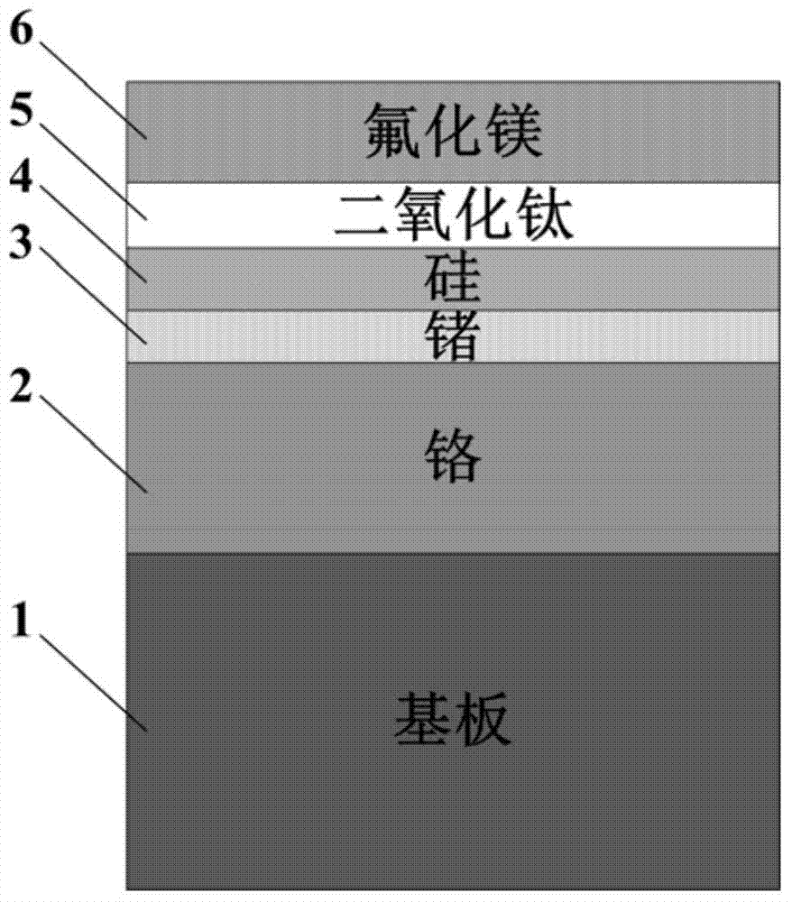
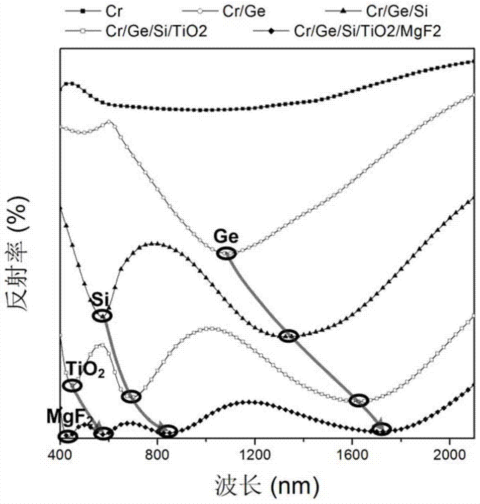
[0041] Embodiment 1: Visible-near-infrared band ultra-broadband absorber, the expected absorption bandwidth is 400nm-1200nm, and the average absorption rate is more than 98%. The absorption spectrum of the absorber sample prepared by the present invention is as follows: Figure 4 As shown in (a), the average absorption rate is above 98.75%. The corresponding base material is a silicon wafer, and the corresponding film materials are sequentially chromium, germanium, silicon, titanium dioxide, and magnesium fluoride. The corresponding film layers of each film layer The thicknesses are 200nm (chromium), 18nm (germanium), 19nm (silicon), 35nm (titanium dioxide), and 80nm (magnesium fluoride).
Embodiment 2
[0042] Embodiment 2: Visible-near-infrared band ultra-broadband absorber, the expected absorption bandwidth is 400nm-2000nm, and the absorption rate of each wavelength is more than 90%. The absorption spectrum of the absorber sample prepared by the present invention is as follows Figure 4 As shown in (b), the average absorption rate is above 97.75%. The corresponding base material is a silicon wafer, and the corresponding film layer materials are sequentially chromium, germanium, silicon, titanium dioxide, and magnesium fluoride. The film corresponding to each film layer The layer thicknesses are 200nm (chromium), 33nm (germanium), 32nm (silicon), 56nm (titanium dioxide), 118nm (magnesium fluoride), respectively.
PUM
| Property | Measurement | Unit |
|---|---|---|
| thickness | aaaaa | aaaaa |
| thickness | aaaaa | aaaaa |
| thickness | aaaaa | aaaaa |
Abstract
Description
Claims
Application Information


