Perovskite-silicon integral cascading and overlapped solar cell and manufacturing method thereof

A technology of stacked solar and solar cells, applied in semiconductor/solid-state device manufacturing, circuits, photovoltaic power generation, etc., can solve problems such as low efficiency, and achieve the goal of accelerating promotion, reducing capital cost investment and resource waste, and efficient distribution and utilization. Effect

Inactive Publication Date: 2015-11-04
NORTH CHINA ELECTRIC POWER UNIV (BAODING)
View PDF6 Cites 20 Cited by
  • Summary
  • Abstract
  • Description
  • Claims
  • Application Information

AI Technical Summary

Problems solved by technology

Although the efficiency of this type of laminated battery is relatively low at present,

Method used


Image

  • Perovskite-silicon integral cascading and overlapped solar cell and manufacturing method thereof
  • Perovskite-silicon integral cascading and overlapped solar cell and manufacturing method thereof
  • Perovskite-silicon integral cascading and overlapped solar cell and manufacturing method thereof

Examples


Example Embodiment

[0037] The following detailed description with reference to the drawings and examples will further illustrate the structure, characteristics and device manufacturing process of the present invention.

[0038] 1. The preparation of crystalline silicon bottom solar cell 2 includes the following steps:

[0039] 1) Single crystal silicon surface texturing

[0040] A single crystal silicon wafer with a thickness of 180±10μm and a size of 15mm×15mm was put into a 5% sodium citrate solution and reacted at 90°C for 5 minutes to remove dirt and damage on the surface of the silicon wafer.

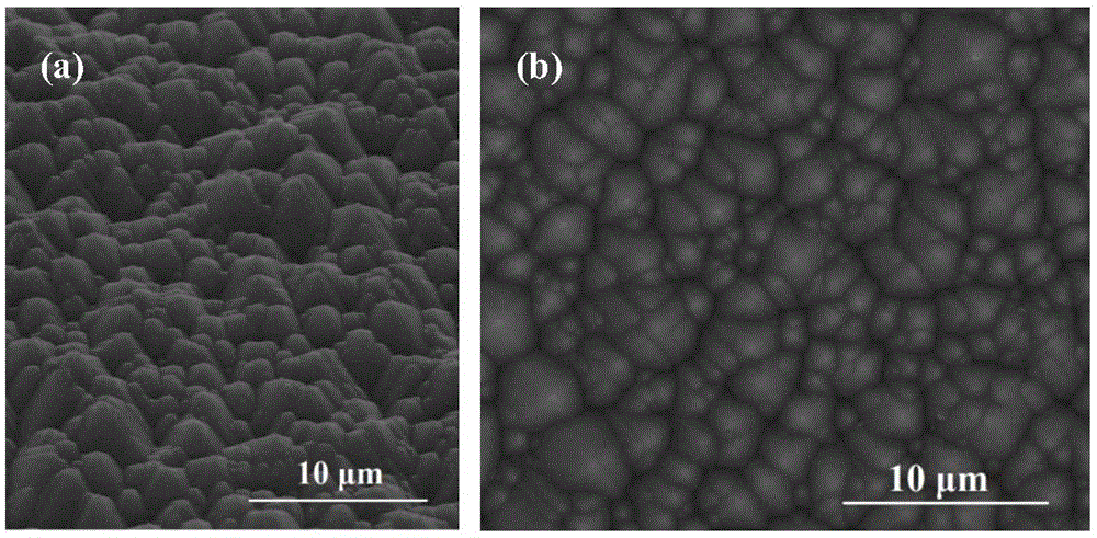
[0041] Put the cleaned silicon wafer into a mixed solution of KOH and isopropanol, where the concentration of KOH is 3%, the volume concentration of isopropanol is 8%, and react at 85°C for 30 minutes to form a uniform surface on the silicon wafer Pyramid structure, such as figure 2 Shown.

[0042] What needs to be emphasized is figure 2 Figures (a) and (b) respectively show the preparation of Si 3 N 4 Scan...


PUM

PropertyMeasurementUnit
Resistivityaaaaaaaaaa
Thicknessaaaaaaaaaa
Sizeaaaaaaaaaa

Abstract

The invention discloses a high-efficiency perovskite-silicon integral cascading and overlapped solar cell and a manufacturing method thereof. The solar cell comprises a back field electrode, a crystalline silicon bottom solar cell, a PEDOT:PSS-TIPD tunnel junction, a fullerene electron transmission layer, a perovskite top solar cell, a 3-hexylthiophene polymer hole transporting layer and a top electrode sequentially from bottom to top. The manufacturing method comprises steps: the back field electrode is manufactured by adopting silk-screen printing, magnetron sputtering or thermal evaporation; according to the crystalline silicon bottom solar cell, after etching is carried out by adopting the traditional crystalline silicon solar cell wet etching method, a liquid source diffusion method is then adopted for manufacturing a pn junction; the tunnel junction is manufactured in a method of combining a chemical synthesis method, a spin coating method and a thermal annealing method; the fullerene electron transmission layer is manufactured by adopting a spin coating method; the perovskite top solar cell is manufactured in a method of combining a chemical synthesis method, a spin coating method and a thermal annealing method; the 3-hexylthiophene polymer hole transporting layer is manufactured in a method of combing the spin coating method and the thermal annealing method; and the top electrode is manufactured by adopting a thermal evaporation method or a magnetron sputtering method.

Description

technical field [0001] The invention belongs to the field of solar cell materials and devices, and in particular relates to a perovskite-silicon integral cascade stacked solar cell and a preparation method thereof. Background technique [0002] In today's increasingly prominent energy problems, photovoltaic power generation technology has attracted much attention. In particular, crystalline silicon solar cells currently account for 86% of the photovoltaic market. Compared with other types of batteries, crystalline silicon solar cells have the advantages of low cost, simple preparation process, and suitable for large-scale production. However, because their efficiency has approached the theoretical limit, it is difficult to achieve a major breakthrough. At present, the highest efficiency of crystalline silicon solar cell laboratory is 24.7%, and the highest efficiency of commercial n-PERT type crystalline silicon solar cell components is 22.02%. [0003] Perovskite solar ce...

Claims


Application Information

Patent Timeline
IPC IPC(8): H01L25/16H01L51/42H01L51/46H01L51/48H01L31/068H01L31/18
CPCY02E10/547Y02E10/549Y02P70/50
Inventor 白一鸣李聪吴云召延玲玲谭占鳌
Owner NORTH CHINA ELECTRIC POWER UNIV (BAODING)
Why Eureka
Try Eureka