

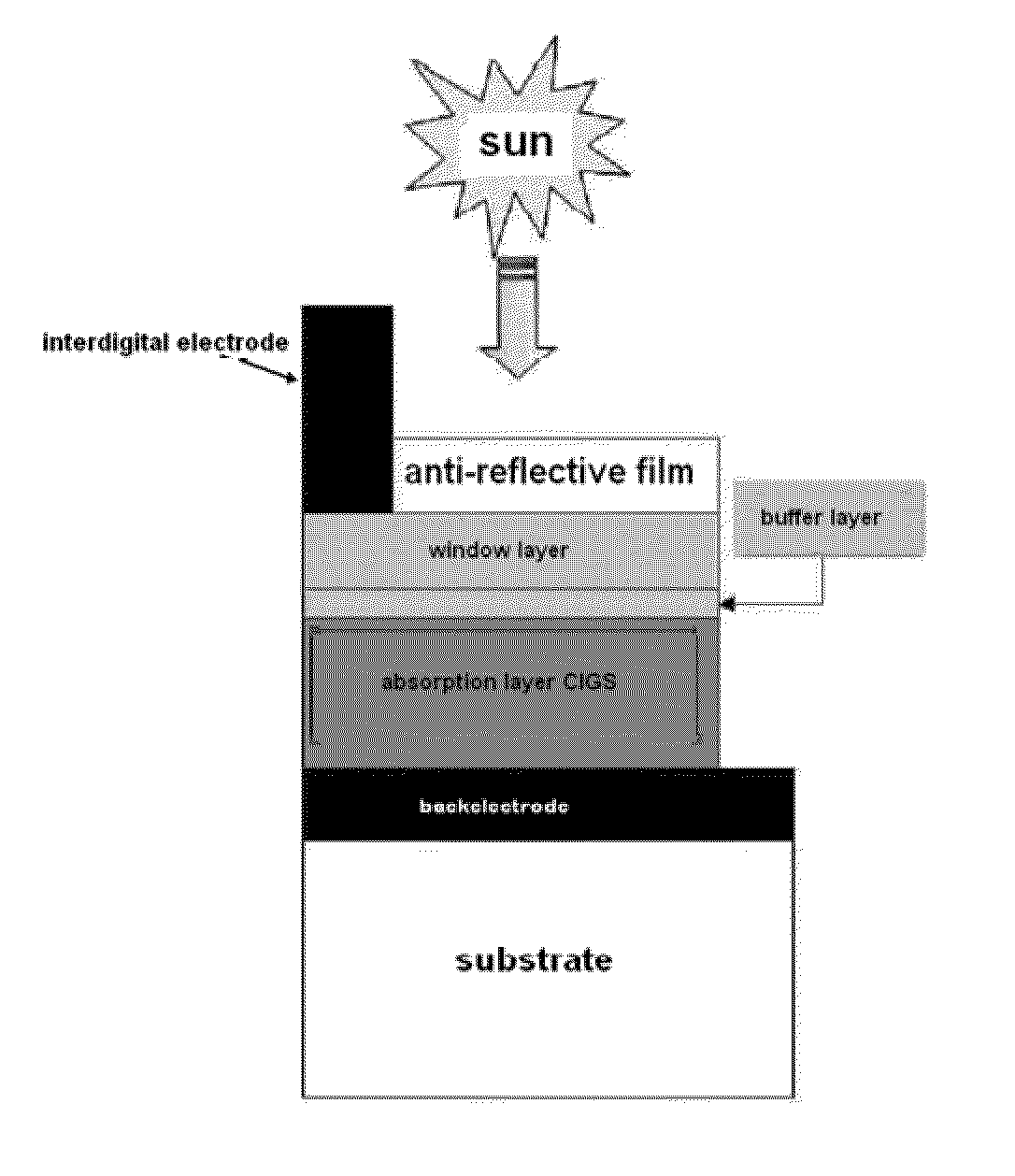
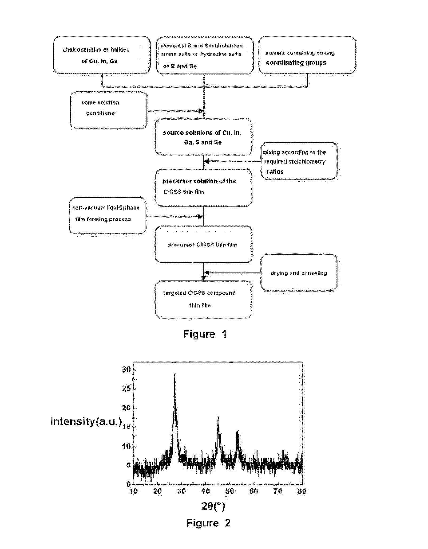
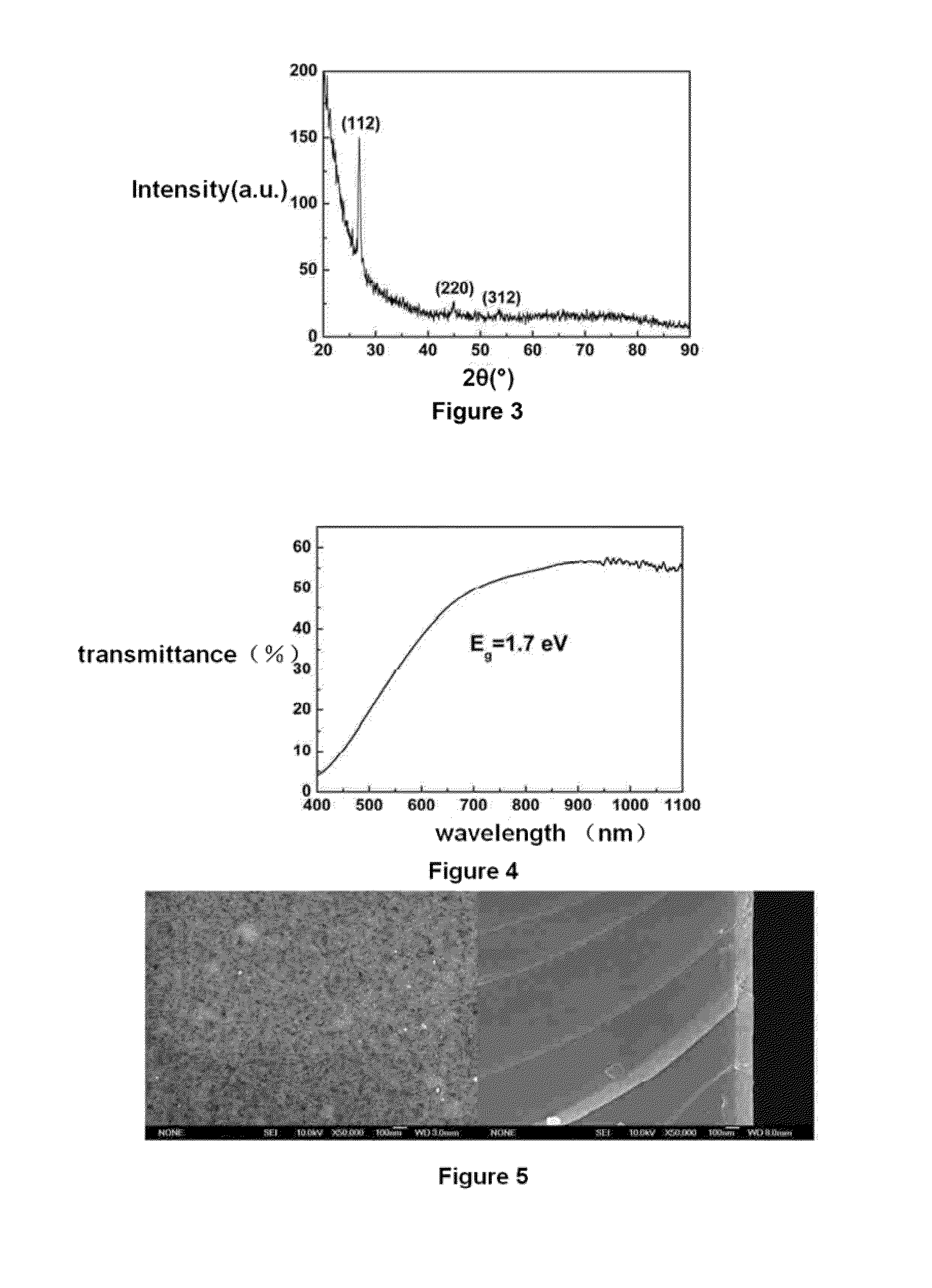
Method for preparing light absorption layer of copper-indium-gallium-sulfur-selenium thin film solar cells
a technology of copper-indiumgallium sulfur and thin film solar cells, which is applied in the field of photovoltaic cell devices, can solve the problems of low yield rate and high production cost, low raw material utilization rate, and difficult to ensure the uniformity of thin films, etc., and achieves low cost, favorable controllability, and simple process
- Summary
- Abstract
- Description
- Claims
- Application Information
AI Technical Summary
Benefits of technology
Problems solved by technology
Method used
Image

Examples
example 1
1. Preparation of the Precursor Solution of CIGSS Thin Film
[0080](a) Preparation of the Solution Comprising Cu and In
[0081]1 mmol Cu2(S,Se), 0.5 mmol In2Se3, 0.2 mmol InI3, 0˜8 mmol S and 0˜8 mmol Se were added into 2˜16 ml mixed solvents composed of methyl hydrazine, ethanolamine and dimethyl sulfoxide, wherein the volume ratio was methyl hydrazine:ethanolamine:dimethyl sulfoxide=1˜3:1˜6:1˜8. The mixture was agitated to produce a clear solution.
[0082](b) Preparation of the Solution Containing Ga
[0083]0.6 mmol Ga2Se3, 0.3 mmol GaBr3, 0.1 mmol Gal3, 0˜8 mmol Se and a trace of Ru powders were added into a 1-8 ml mixed solvents composed of methyl hydrazine, ethanolamine and dimethyl sulfoxide, wherein the volume ratio was methyl hydrazine:ethanolamine:dimethyl sulfoxide=1˜3:1˜6:1˜8. The mixture was sufficiently agitated and filtrated through a 0.2 μm filter to produce a clear solution comprising Ga.
[0084](c) Preparation of the Precursor Solution of CIGSS Thin Film
[0085]Above solutions ...
example 2
1. Preparation of the Precursor Solution of CIGSS Thin Film
[0098](a) Preparation of the solution containing Cu
[0099]1 mmol CuI was added into 2˜16 ml ethylene glycol. The mixture was sufficiently agitated to produce a clear solution.
[0100](b) Preparation of the Solution Containing In
[0101]1 mmol indium iodide and 0˜8 mmol Se were added into 1˜8 ml mixed solvents composed of methyl hydrazine and n-butanol, wherein the volume ratio was methyl hydrazine:n-butanol=1˜3:1˜8. The mixture was sufficiently agitated and filtrated through a 0.2 μM filter to produce a clear solution containing In.
[0102](c) Preparation of the Solution Containing Ga
[0103]1 mmol GaI3 and 4˜8 mmol Se were added into 1˜8 ml mixed solvents composed of methyl hydrazine and n-butanol, wherein the volume ratio was methyl hydrazinem-butanol=1˜3:1˜8. The mixture was sufficiently agitated and filtrated through a 0.2 μm filter to produce a clear solution containing Ga.
[0104](d) Preparation of the Precursor Solution of CIGSS...
example 3
1. Preparation of the Precursor Solution of CIGSS Thin Film
[0112](a) Preparation of the Solution Containing Cu and Se
[0113]1 mmol CuCl was added into 2˜16 ml mixed solvents composed of ethylene diamine, dodecyl mercaptan and N,N-dimethyl formamide, wherein volume ratio was ethylene diamine:dodecyl mercaptan:N,N-dimethyl formamide=1˜8:1˜3:1˜6. The mixture was sufficiently agitated to produce a clear solution containing copper. Then 2-6 mmol Se was added into 4-16 ml ethylene diamine, and the mixture was sufficiently agitated and refluxed under 80° C. to produce a clear solution of selenium in ethylene diamine. The ethylene diamine solution of selenium was added in above solution containing Cu under agitation to produce the solution containing Cu and Se.
[0114](b) Preparation of the Solution Containing In
[0115]1 mmol indium iodide InI3 was added into 2˜16 ml mixed solvents composed of ethanol and isopropanol, wherein the volume ratio was ethanol isopropanol=1˜3:1˜6. The mixture was suf...
PUM
 Abstract
Description
Claims
Application Information