

Package structure for silicon-based module and package method for silicon-based module
A packaging structure, silicon-based technology, applied in the direction of electrical components, electrical solid devices, circuits, etc., can solve the problems of reduced current carrying capacity, heat dissipation can not meet the demand, complicated packaging structure, etc., to achieve simple packaging structure, ensure thermal conductivity, Overcome the effect of complicated packaging structure and complicated process
- Summary
- Abstract
- Description
- Claims
- Application Information
AI Technical Summary
Problems solved by technology
Method used
Image

Examples
Embodiment 1
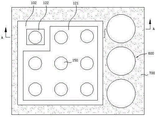
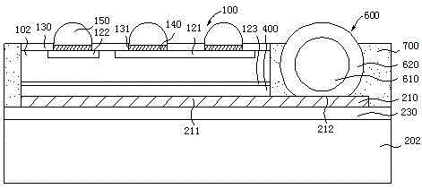
[0063] Embodiment one, see figure 1 and figure 2
[0064] figure 1 It is a schematic diagram of the front structure of the packaging structure of a silicon-based module of the present invention, figure 2 for figure 1 A-A cross-sectional schematic diagram. Depend on figure 1 and figure 2It can be seen that the packaging structure of the silicon-based module of the present invention includes a silicon-based chip 100, metal core solder balls 600, and a silicon-based carrier 202. The cross-sectional size of the silicon-based carrier 202 is larger than that of the silicon-based chip 100, and the silicon-based The chip 100 and the metal core solder ball 600 are disposed above the silicon-based carrier 202 . The inner core of the metal core solder ball 600 is a spherical metal core 610. The material of the metal core 610 is generally copper, or a layer of metal nickel layer or nickel / gold layer is wrapped on the outside of the copper core, and the outermost layer of the...
PUM
 Abstract
Description
Claims
Application Information