
Thin film crystalline silicon perovskite heterojunction solar cell and preparation method thereof

A solar cell and perovskite technology, applied in circuits, electrical components, electrical solid devices, etc., can solve the problems of insufficient stability, poor photoelectric conversion performance of perovskite solar cells, and large usage.

Active Publication Date: 2018-01-30
HEBEI UNIV OF TECH
View PDF9 Cites 2 Cited by
  • Summary
  • Abstract
  • Description
  • Claims
  • Application Information

AI Technical Summary

Problems solved by technology

[0004] The technical problem to be solved by the present invention is to provide a thin-film crystalline silicon perovskite heterojunction solar cell and a preparation method thereof, which is a solar cell and a preparation method using a heterojunction composed of thin-film crystalline silicon and perovskite. It overcomes the shortcomings of the existing ordinary perovskite solar cells due to the lack of stability and high manufacturing cost due to the use of organic hole transport layer materials, and overcomes the perovskite solar cells that use bulk crystalline silicon materials as hole transport materials. The defect of using a large amount of silicon materials for cells, and also overcomes the defect of poor photoelectric conversion performance of perovskite solar cells using amorphous silicon and microcrystalline silicon thin films as hole transport layers

Method used


Image

  • Thin film crystalline silicon perovskite heterojunction solar cell and preparation method thereof

Examples


Embodiment 1

[0060] The first step is to prepare a P-type thin film crystalline silicon hole transport layer on a transparent conductive substrate:

[0061] Use a P-type single crystal silicon wafer coated with a layer of corrosion-resistant metal on the back as the anode, and use platinum as the cathode. anodic oxidation with an electric current, corrode the P-type single crystal silicon wafer by electrochemical method, and form a porous silicon structure on the surface of the single crystal silicon wafer, and then form the single crystal silicon wafer with the porous silicon structure in H 2 Annealing at 200°C to 550°C in the atmosphere, during the annealing process, the holes in the small porosity layer on the surface of the single crystal silicon wafer will gradually close to form a quasi-single crystal layer as a template for epitaxial devices. The P-type thin film crystalline silicon film is epitaxially formed on the layer, and the formed P-type crystalline silicon film is transferre...

Embodiment 2

[0081] The first step is to prepare a P-type thin film crystalline silicon hole transport layer on a transparent conductive substrate:

[0082] With a P-type single crystal silicon wafer coated with a layer of corrosion-resistant metal on the back as the anode and platinum as the cathode, in a hydrofluoric acid ethanol solution with a volume ratio of hydrofluoric acid: absolute ethanol = 1:1, the size is 4.5 The current of A is anodized, and the P-type single crystal silicon wafer is corroded by an electrochemical method to form a porous silicon structure on the surface of the single crystal silicon wafer, and then the single crystal silicon wafer with a porous silicon structure is formed in H 2 Annealing at 200°C to 550°C in the atmosphere, during the annealing process, the holes in the small porosity layer on the surface of the single crystal silicon wafer will gradually close to form a quasi-single crystal layer as a template for epitaxial devices. The P-type thin film crys...

Embodiment 3

[0102] The first step is to prepare a P-type thin film crystalline silicon hole transport layer on a transparent conductive substrate:

[0103] With a P-type single crystal silicon wafer coated with a layer of corrosion-resistant metal on the back as the anode, and platinum as the cathode, in a hydrofluoric acid ethanol solution with a volume ratio of hydrofluoric acid: absolute ethanol = 1:1, a size of 7.5 The current of A is anodized, and the P-type single crystal silicon wafer is corroded by an electrochemical method to form a porous silicon structure on the surface of the single crystal silicon wafer, and then the single crystal silicon wafer with a porous silicon structure is formed in H 2 Annealing at 200°C to 550°C in the atmosphere, during the annealing process, the holes in the small porosity layer on the surface of the single crystal silicon wafer will gradually close to form a quasi-single crystal layer as a template for epitaxial devices. The P-type thin film cryst...


PUM

PropertyMeasurementUnit
thicknessaaaaaaaaaa
thicknessaaaaaaaaaa
thicknessaaaaaaaaaa

Abstract

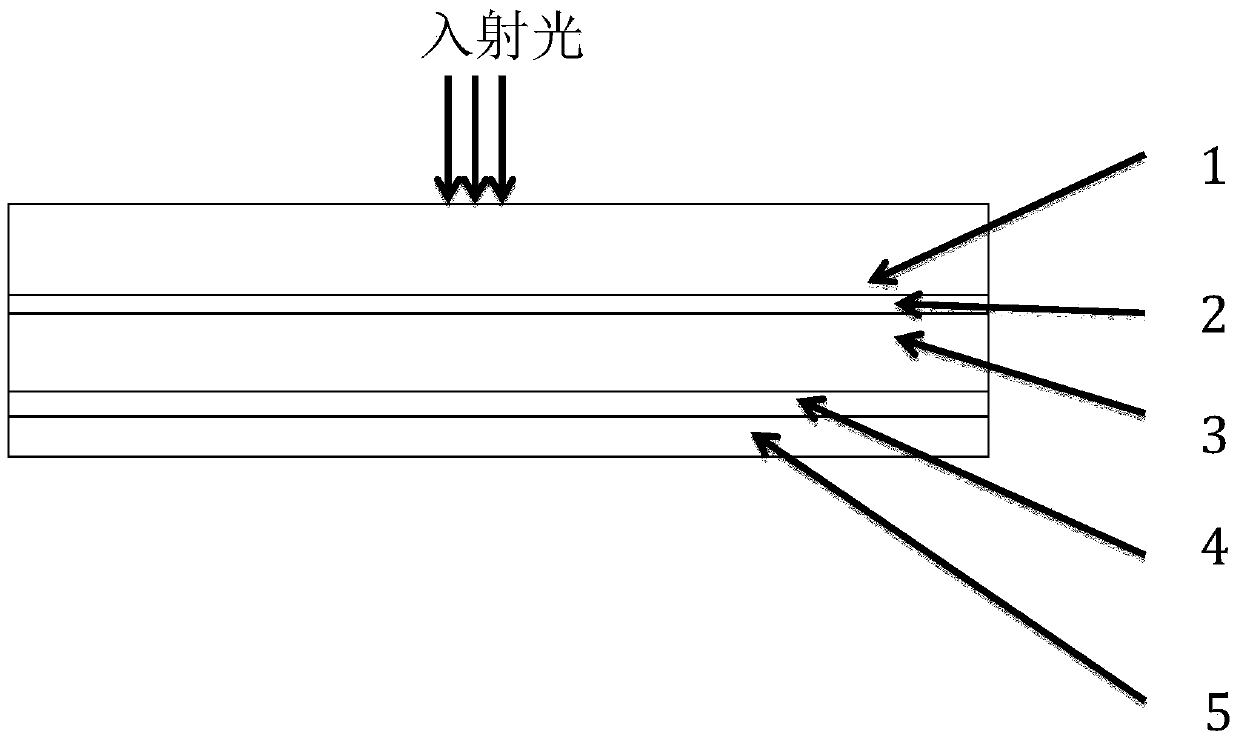
The invention relates to a thin-film crystalline silicon perovskite heterojunction solar cell and a preparation method thereof, which relate to a semiconductor device specially suitable for converting light energy into electrical energy, which consists of a transparent conductive substrate, a P-type thin-film crystalline silicon hole transport layer, and a perovskite The light absorbing layer, the electron transport layer made of dense titanium dioxide and the back electrode are composed of the perovskite light absorbing layer and the P-type thin film crystalline silicon hole transport layer with matching energy levels; the composition method is: P-type thin film crystal The silicon hole transport layer is placed on the transparent conductive substrate, the perovskite light absorbing layer is placed on the top of the P-type thin film crystalline silicon hole transport layer, and the perovskite light absorbing layer and the P-type thin film crystalline silicon hole transport layer form a thin film In the crystalline silicon perovskite heterojunction, the electron transport layer composed of dense titanium dioxide is placed on the perovskite light absorbing layer, and the back electrode is placed on the electron transport layer composed of dense titanium dioxide. It overcomes the shortcomings of the existing perovskite solar cells, such as insufficient stability, high manufacturing cost or large amount of silicon materials used.

Description

technical field [0001] The technical solution of the invention relates to a semiconductor device specially suitable for converting light energy into electric energy, specifically a thin-film crystal silicon perovskite heterojunction solar cell and a preparation method thereof. Background technique [0002] Compared with crystalline silicon cells, which are difficult to further reduce the manufacturing cost of crystalline silicon materials, the perovskite material CH 3 NH 3 wxya 3 (X=Cl, Br, or I) is the main light-absorbing layer of solar cells (hereinafter referred to as perovskite solar cells) with a photoelectric conversion efficiency of more than 20%, and has the advantages of thin film, room temperature solution preparation, and no rare elements. The characteristics of manufacturing cost have great application prospects. In perovskite solar cells with various structures, the P-type bulk silicon material of traditional monocrystalline silicon and polycrystalline silic...

Claims


Application Information

Patent Timeline
Patent Type & Authority Patents(China)
IPC IPC(8): H01L51/00H01L51/52H01L51/54H01L51/56H10K99/00
CPCH10K99/00H10K50/14H10K50/80H10K2102/00H10K2102/302H10K71/00
Inventor 田汉民金慧娇毕文刚花中秋杨瑞霞戎小莹张天王伟
Owner HEBEI UNIV OF TECH
Learn More