

Gecko-inspired biomimetic dry glue and preparation method thereof
A technology for gecko and dry glue, applied in the field of bionic gecko dry glue and its preparation, can solve the problems of difficult processing of regular and ordered structures and high cost
- Summary
- Abstract
- Description
- Claims
- Application Information
AI Technical Summary
Problems solved by technology
Method used
Image

Examples
Embodiment 1
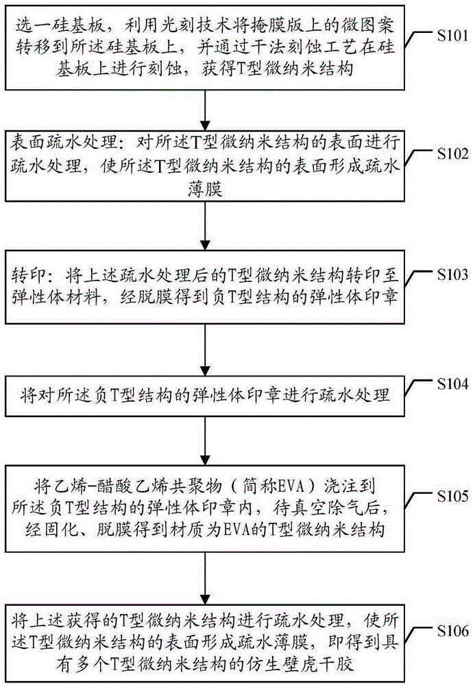
[0074] See attached figure 1 The flow chart of the preparation method of the bionic gecko dry glue, the preparation method of a kind of bionic gecko dry glue provided in this embodiment comprises the following steps:
[0075] S101. Preparation of micro-nano structure: select a silicon substrate, which is a silicon substrate with a thermally grown silicon dioxide film with a thickness of 300 nm on the surface, spin-coat photoresist on the above-mentioned silicon substrate, expose and develop, and The micro-scale pattern on the designed mask is transferred to the surface of the spin-coated photoresist; the pattern on the photoresist is further transferred to SiO2 by reactive ion etching 2 thin surface, specifically using photoresist as a mask, using CF 4 or CHF 3 Gas plasma etch SiO 2 thin film until the silicon surface is exposed, then wash off the photoresist with a stripper or acetone, and pass through O 2 plasma cleaning;
[0076] The silicon substrate is then etched b...
Embodiment 2
[0090] A preparation method of bionic gecko dry glue, comprising the following steps:
[0091] (1) Preparation of micro-nano structure: choose a silicon substrate, the silicon substrate is a silicon substrate with thermal growth on the surface and a silicon dioxide film with a thickness of 300nm, spin-coat photoresist on the above-mentioned silicon substrate, expose, develop, Transfer the micro-scale pattern on the designed mask to the surface of the spin-coated photoresist; use reactive ion etching to further transfer the pattern on the photoresist to SiO 2 thin surface, specifically using photoresist as a mask, using CF 4 or CHF 3 Gas plasma etch SiO 2 thin film until the silicon surface is exposed, then wash off the photoresist with a stripper or acetone, and pass through O 2 plasma cleaning;
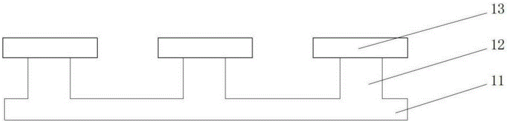
[0092] Then, the silicon substrate is etched by a vapor phase etching process until a T-shaped micro-nano structure is obtained, as follows: using XeF 2 The silicon surface is t...
Embodiment 3
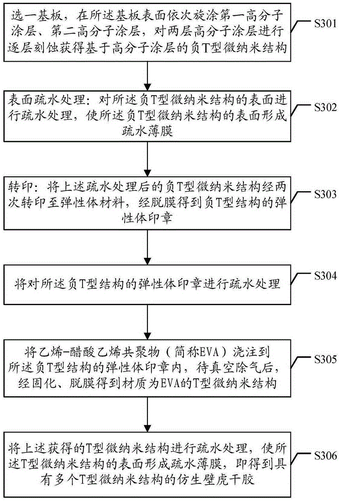
[0102] See attached image 3 The flow chart of the preparation method of the bionic gecko dry glue, the preparation method of a kind of bionic gecko dry glue provided in this embodiment comprises the following steps:
[0103] S301. Prepare micro-nano structure: select a silicon substrate, spin-coat AR5460 and SU8-T3035 photoresist on the surface of the substrate sequentially as the first polymer coating and the second polymer coating, and then use SU-8 to develop agent to develop the second polymer coating to obtain specific micro or nano patterns;
[0104] Use AR300 developer to etch the first polymer coating through the developed second polymer coating; form a negative T-shaped micro-nano structure on the second polymer coating and the first polymer coating;
[0105] S302. Surface hydrophobic treatment: perform hydrophobic treatment on the surface of the above-mentioned negative T-shaped micro-nano structure, so that the surface of the negative T-shaped micro-nano structure...
PUM
| Property | Measurement | Unit |
|---|---|---|
| size | aaaaa | aaaaa |
| height | aaaaa | aaaaa |
| length | aaaaa | aaaaa |
Abstract
Description
Claims
Application Information