Preparation method of semiconductor device

A semiconductor and device technology, which is applied in the field of semiconductor device preparation, can solve the problems of increased production cost and complicated process flow, and achieve the effects of low cost, simplified silicon oxide filling, and improved alignment accuracy

Active Publication Date: 2016-01-13
SHANGHAI HUALI MICROELECTRONICS CORP
View PDF6 Cites 6 Cited by
  • Summary
  • Abstract
  • Description
  • Claims
  • Application Information

AI Technical Summary

Problems solved by technology

[0007] In view of the above-mentioned problems, the present invention discloses a method for preparing a semiconductor device to overcome the need in the prior art to make up for the height difference of the wafer surface by chemical vapor deposition, chemical mechanical polishing and wet etching on the zero layer. Alignment marks are filled with silicon oxide, which complicates the process and increases production costs

Method used


Image

  • Preparation method of semiconductor device
  • Preparation method of semiconductor device
  • Preparation method of semiconductor device

Examples


Embodiment Construction

[0028] The present invention will be further described below in conjunction with the accompanying drawings and specific embodiments, but not as a limitation of the present invention.

[0029] Figure 1-4 is a schematic flow chart of a method for preparing a semiconductor device in an embodiment of the present invention; as Figure 1-4 Shown:

[0030] This embodiment relates to a method for preparing a semiconductor device, which can be applied to the preparation process of a CMOS image sensor (CIS), and specifically includes the following steps:

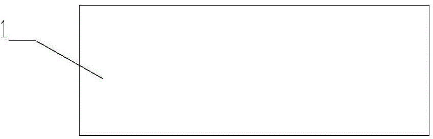
[0031] Step S1, provide a semiconductor substrate 1, in the embodiment of the present invention, the semiconductor substrate 1 is a silicon wafer, such as figure 1 structure shown.

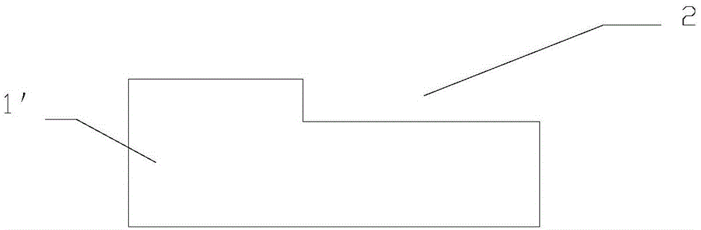
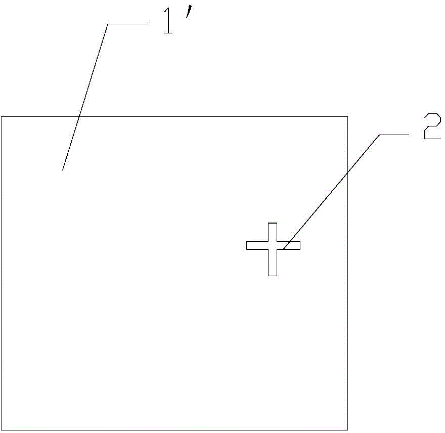
[0032] Step S2, etching a zero-layer alignment mark (AlignmentMark) 2 on the upper surface of the semiconductor substrate 1. In an embodiment of the present invention, the step of etching the zero-layer alignment mark 2 is specifically, spin coating A...


PUM


Abstract

The invention discloses a preparation method of a semiconductor device. According to the invention, in the process of forming a polysilicon gate through etching a polysilicon layer, an etching area is ensured to be kept away from a zero layer alignment identifier, the polysilicon layer formed by etching is still enabled to cover the zero layer alignment identifier, the height difference in chip caused by the zero layer alignment identifier is introduced into the polysilicon gate, and then the height difference is eliminated in the follow-up interlayer dielectric filling and flattening process, thereby simplifying the steps of silicon oxide filling, flattening, wet etching and the like of the zero layer alignment identifier in a traditional zero layer alignment technology through optimizing the design of the polysilicon layer and the depth of the zero layer alignment identifier, realizing a semiconductor preparation technology without shallow trench isolation, and being simple in technological process and low in cost.

Description

technical field [0001] The invention relates to the technical field of semiconductor manufacturing, in particular to a method for preparing a semiconductor device. Background technique [0002] In the field of semiconductor technology, the shallow trench isolation technology can effectively reduce and eliminate the parasitic field effect transistor effect in semiconductor planar manufacturing. Its basic process is to use dry etching to etch an isolation trench with a depth of 0.1um to 0.5um on the surface of the silicon wafer, then grow a linear oxide layer on the surface of the isolation trench, fill the silicon oxide with chemical vapor deposition, and use chemical mechanical Polishing to achieve planarization. However, for some special products, such as CMOS image sensors, shallow trench isolation technology will introduce many surface energy levels and lattice damage, which will adversely affect some key parameters of the product, including dark current and white pixels...

Claims


Application Information

Patent Timeline
Patent Type & Authority Applications(China)
IPC IPC(8): H01L21/28H01L27/146
Inventor 范晓陈昊瑜王奇伟
Owner SHANGHAI HUALI MICROELECTRONICS CORP
Why Eureka
Try Eureka