A passivation method for boron emitter of n-type crystalline silicon cell

A crystalline silicon battery and emitter technology, which is applied in the direction of circuits, electrical components, sustainable manufacturing/processing, etc., can solve the problems of passivation performance decline, low utilization rate of chemical materials, low material utilization rate, etc., and achieve equipment cost and Low cost of consumables, ease of mass production, effects of economical process methods

Active Publication Date: 2017-05-31
中国东方电气集团有限公司
View PDF4 Cites 0 Cited by
  • Summary
  • Abstract
  • Description
  • Claims
  • Application Information

AI Technical Summary

Problems solved by technology

However, the traditional ALD equipment itself has the disadvantages of slow growth rate, low material utilization rate and expensive equipment, which is not compatible with the large-scale production of solar cell industry. Only with the improvement of technology and the reduction of equipment cost, continuous deposition ALD equipment and Al 2 o 3 Thin film passivation process can enter solar cell production
The α-Si:H film prepared by PECVD also has the problem of low chemical material utilization and the H loss passivation performance of the α-Si:H film after sintering.

Method used


Image

  • A passivation method for boron emitter of n-type crystalline silicon cell
  • A passivation method for boron emitter of n-type crystalline silicon cell

Examples


Embodiment 1

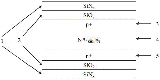
[0020] like figure 1 Shown, a kind of passivation method of boron emitter of N-type crystalline silicon battery comprises the following steps:

[0021] (1) Use N-type monocrystalline silicon wafers as the substrate, with a resistivity of 1-12 W cm and a thickness of 170-200 mm. The silicon wafers are cleaned to remove the damaged layer on the surface, and the silicon wafers are treated with alkaline solution. Texturing treatment;

[0022] (2) The boron emitter P+ layer is prepared by doping the silicon wafer with boron on one side of the silicon wafer through high-temperature boron diffusion;

[0023] (3) Remove the borosilicate glass on the surface and the diffusion diffraction layer on the back by wet etching, and prepare a phosphorus diffusion mask layer on the boron emitter P+ layer;

[0024] (4) Use a tube furnace to diffuse phosphorus on the other side of the silicon wafer to form an N+ layer, and use chemical etching to remove the surface phosphosilicate glass layer a...

Embodiment 2

[0028] like figure 1 Shown, a kind of passivation method of boron emitter of N-type crystalline silicon battery comprises the following steps:

[0029] (1) Use N-type monocrystalline silicon wafers as the substrate, with a resistivity of 1-12 W cm and a thickness of 170-200 mm. The silicon wafers are cleaned to remove the damaged layer on the surface, and the silicon wafers are treated with alkaline solution. Texturing treatment;

[0030] (2) The boron emitter P+ layer is prepared by doping the silicon wafer with boron on one side of the silicon wafer through high-temperature boron diffusion;

[0031] (3) Remove the borosilicate glass on the surface and the diffusion diffraction layer on the back by wet etching, perform phosphorus doping on the other side of the silicon wafer by implantation, and form a phosphorus-doped N+ layer after annealing;

[0032] (4) Put the silicon wafer in (3) into an oxidation furnace for oxidation passivation treatment in a high-purity oxygen atm...


PUM

PropertyMeasurementUnit
thicknessaaaaaaaaaa
thicknessaaaaaaaaaa

Abstract

The invention provides a passivation method for an N-type crystalline silicon cell boron emitter. The passivation steps are listed as follows: a phosphor doped N+ layer and a boron emitter P+ layer are respectively formed on the two surfaces of an N-type silicon substrate; then oxidation and passivation processing is performed on the N-type silicon substrate, and a silicon oxide film is respectively generated on the phosphor doped N+ layer and the boron emitter P+ layer; and finally a SiNx film is deposited on the silicon oxide film of the two surfaces of the N-type silicon substrate. A silicon dioxide and silicon nitride laminated film acts as the passivation film of the boron emitter, wherein silicon dioxide is prepared and generated through low-temperature dry oxidation, thickness is 2-10nm, and silicon nitride is prepared by a PECVD method. The passivation film system preparation technology is relatively simple, preparation process controllability is high, equipment cost is low and consumable cost is low so as to be compatible with current crystalline silicon cell manufacturing production line equipment and suitable for large-scale industrial production.

Description

technical field [0001] The invention relates to the technical field of solar cell production, in particular to a passivation method for a boron emitter of an N-type crystalline silicon cell. Background technique [0002] At present, crystalline silicon cells are the mainstream products in the solar cell market, and crystalline silicon solar cells can be divided into P-type crystalline silicon cells and N-type crystalline silicon cells in terms of material and substrate types. Compared with P-type monocrystalline silicon cells, N-type monocrystalline silicon cells have the characteristics of small light-induced attenuation, good resistance to metal impurity pollution, and long diffusion length of minority carriers, and have great potential in improving efficiency. [0003] For N-type crystalline silicon cells with a simple structure, the preparation process is usually texture->boron diffusion->phosphorus diffusion / implantation->passivation->anti-reflection film de...

Claims


Application Information

Patent Timeline
Patent Type & Authority Patents(China)
IPC IPC(8): H01L31/18
CPCH01L31/1868Y02P70/50
Inventor 张中伟廖亚琴张世勇
Owner 中国东方电气集团有限公司
Why Eureka
Try Eureka