Passivation method for N-type crystalline silicon cell boron emitter
A crystalline silicon cell and emitter technology, which is applied in the direction of circuits, electrical components, sustainable manufacturing/processing, etc., can solve the problems of decreased passivation performance, low utilization rate of chemical materials, low material utilization rate, etc., and achieves equipment cost and Low cost of consumables, ease of mass production, effects of economical process methods
- Summary
- Abstract
- Description
- Claims
- Application Information
AI Technical Summary
Problems solved by technology
Method used
Image
Examples
Embodiment 1
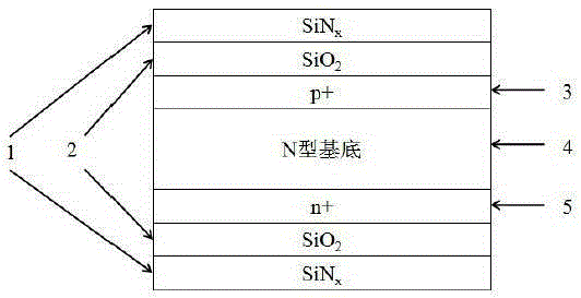
[0020] Such as figure 1 Shown, a kind of passivation method of boron emitter of N-type crystalline silicon battery comprises the following steps:
[0021] (1) Use N-type monocrystalline silicon wafers as the substrate, the resistivity is 1~12W cm, and the thickness is 170~200mm. The silicon wafers are cleaned to remove the damaged layer on the surface, and the silicon wafers are textured with alkaline solution. deal with;
[0022] (2) The boron emitter P+ layer is prepared by doping the silicon wafer with boron on one side of the silicon wafer through high-temperature boron diffusion;
[0023] (3) Remove the borosilicate glass on the surface and the diffusion diffraction layer on the back by wet etching, and prepare a phosphorus diffusion mask layer on the boron emitter P+ layer;
[0024] (4) Use a tube furnace to diffuse phosphorus on the other side of the silicon wafer to form an N+ layer, and use chemical etching to remove the surface phosphosilicate glass layer and the d...
Embodiment 2
[0028] Such as figure 1 Shown, a kind of passivation method of boron emitter of N-type crystalline silicon battery comprises the following steps:
[0029] (1) Use N-type monocrystalline silicon wafers as the substrate, the resistivity is 1~12W cm, and the thickness is 170~200mm. The silicon wafers are cleaned to remove the damaged layer on the surface, and the silicon wafers are textured with alkaline solution. deal with;
[0030] (2) The boron emitter P+ layer is prepared by doping the silicon wafer with boron on one side of the silicon wafer through high-temperature boron diffusion;
[0031] (3) Remove the borosilicate glass on the surface and the diffusion diffraction layer on the back by wet etching, perform phosphorus doping on the other side of the silicon wafer by implantation, and form a phosphorus-doped N+ layer after annealing;
[0032] (4) Put the silicon wafer in (3) into an oxidation furnace for oxidation passivation treatment in a high-purity oxygen atmosphere....
PUM
| Property | Measurement | Unit |
|---|---|---|
| thickness | aaaaa | aaaaa |
| thickness | aaaaa | aaaaa |
Abstract
Description
Claims
Application Information

