FD-GOI tunneling field effect transistor with abrupt tunneling junction and manufacturing method
A technology of tunneling field effect and tunneling junction, which is applied in semiconductor/solid-state device manufacturing, diodes, semiconductor devices, etc., can solve the problems of subthreshold slope theoretical value degradation and small driving current, and achieve suppression of bipolar effect and parasitic Effect of low capacitance and reduced subthreshold slope
- Summary
- Abstract
- Description
- Claims
- Application Information
AI Technical Summary
Problems solved by technology
Method used
Image

Examples
Embodiment 1
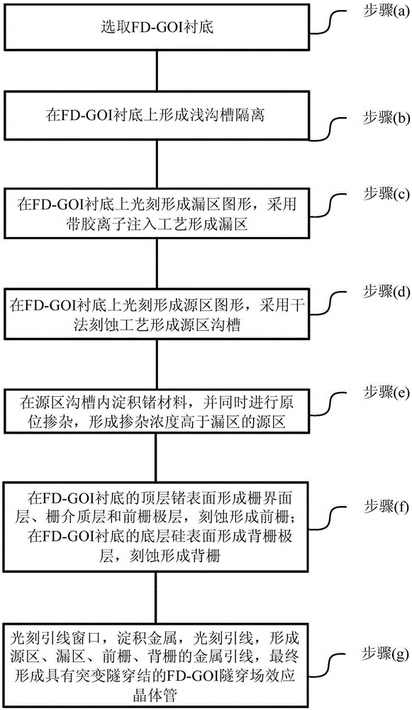
[0055] See figure 1 , figure 1 It is a flowchart of a method for preparing an FD-GOI tunneling field effect transistor with a sudden tunnel junction according to an embodiment of the present invention, and the method includes the following steps:
[0056] Step (a), selecting a fully depleted germanium-on-insulator (Fully Depleted Germanium-On-Insulator, referred to as FD-GOI) substrate;
[0057] Step (b), forming shallow trench isolation on the FD-GOI substrate by an etching process;
[0058] Step (c), forming a drain region pattern by photolithography on the FD-GOI substrate, and forming a drain region by using an ion implantation process with glue;
[0059] Step (d), forming a source region pattern by photolithography on the FD-GOI substrate, and forming a source region trench by a dry etching process;
[0060] Step (e), depositing germanium material in the trench of the source region, and performing in-situ doping at the same time, forming a source region with a higher...
Embodiment 2
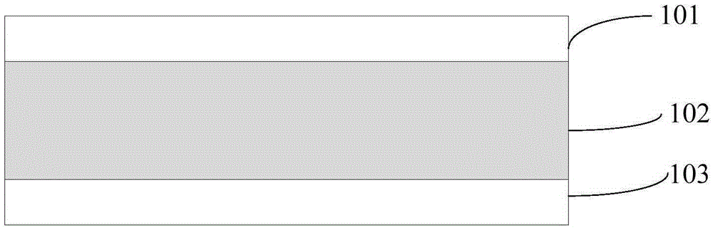
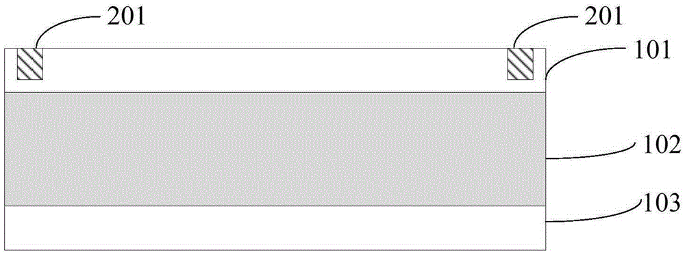
[0095] See Figure 2a-Figure 2h It is a schematic diagram of a method for preparing a FD-GOI tunneling field-effect transistor with a sudden tunnel junction according to an embodiment of the present invention; the specific steps are as follows:
[0096] (1) Select the FD-GOI substrate. Such as Figure 2a As shown, the FD-GOI substrate includes a top layer of germanium 101 , a buried oxide layer 102 such as a buried layer of silicon dioxide, and a bottom layer of silicon 103 .
[0097] The reason for using the FD-GOI substrate is that the Ge material has a small bandgap, high tunneling probability, high carrier mobility, and good velocity characteristics, which is conducive to improving the driving current of the tunneling field effect transistor; the GOI substrate formed Semiconductor devices have the advantages of low power consumption, high speed, high integration density, strong anti-interference ability, strong anti-irradiation ability, and simple process, which can prov...
Embodiment 3
[0127] See image 3 , image 3 It is a schematic flow chart of a method for preparing an FD-GOI tunneling field-effect transistor with an abrupt tunneling junction according to an embodiment of the present invention, to prepare an N-type FD-GOI tunneling field-effect transistor with an abrupt tunneling junction with a channel length of 45 nm. Taking the transistor as an example to describe in detail, the specific steps are as follows:
[0128] 1. Select FD-GOI substrate
[0129] The crystal orientation of the FD-GOI substrate can be (100) or (110) or (111), without any limitation here. In addition, the doping type of the FD-GOI substrate 101 can be N-type or It is P-type, and the doping concentration is, for example, 10 14 ~10 17 cm -3 , the thickness of the top Ge layer is, for example, 20-100 nm, preferably 20 nm.
[0130] 2. Shallow trench isolation formation
[0131] 2.1 Form the first protective layer on the FD-GOI substrate.
[0132] First, two layers of materials ...
PUM
 Abstract
Description
Claims
Application Information
 - R&D
- Intellectual Property
- Life Sciences
- Materials
- Tech Scout
- Unparalleled Data Quality
- Higher Quality Content
- 60% Fewer Hallucinations
Browse by: Latest US Patents, China's latest patents, Technical Efficacy Thesaurus, Application Domain, Technology Topic, Popular Technical Reports.
© 2025 PatSnap. All rights reserved.Legal|Privacy policy|Modern Slavery Act Transparency Statement|Sitemap|About US| Contact US: help@patsnap.com