Preparation method of fast recovery diode

A technology for recovering diodes and anode surfaces, applied in semiconductor/solid-state device manufacturing, electrical components, circuits, etc., can solve problems such as oversize, chip overheating, FRD softness factor S reduction, etc.

Active Publication Date: 2016-02-24
ZHUZHOU CRRC TIMES SEMICON CO LTD
View PDF3 Cites 5 Cited by
  • Summary
  • Abstract
  • Description
  • Claims
  • Application Information

AI Technical Summary

Problems solved by technology

[0004] Most of the IGCT supporting fast recovery diodes on the market adopt a full crimping structure. The full crimping fast recovery diode (FRD) has the following disadvantages: due to structural limitations, the heat dissipation capacity of the device is limited, and during the reverse recovery process , it is easy to cause local overheating of the chip, resulting in chip failure. When the power of the application circuit continues to increase, the failure rate of the full-press FRD increases sharply; the full-press FRD generally applies a large dose of electron radiation to redu

Method used


Image

  • Preparation method of fast recovery diode
  • Preparation method of fast recovery diode
  • Preparation method of fast recovery diode

Examples


Embodiment 1

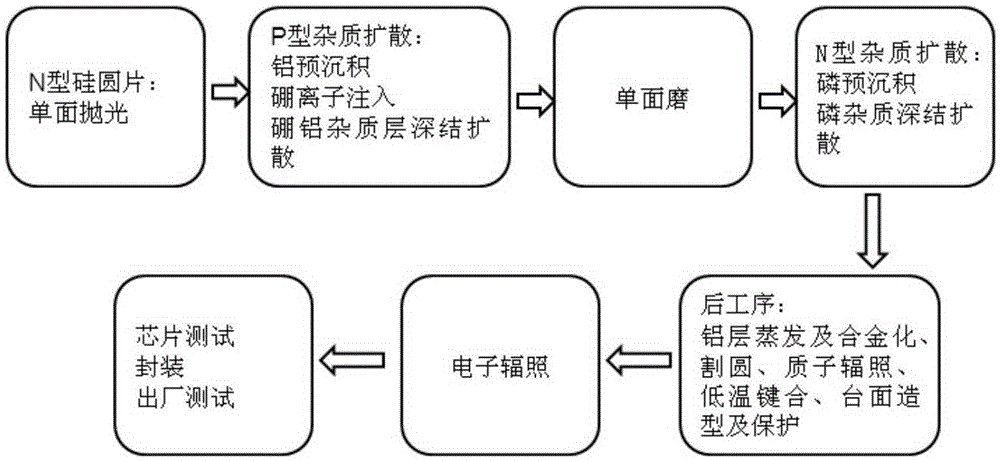
[0071] Adopt manufacturing method described in the present invention to manufacture IGCT matching FRD (ZK X 2000-45). Including the following steps:

[0072] 1. Take an N-type silicon wafer with a diameter of 76.2mm, a thickness of 0.80mm, a crystal orientation of , and a resistivity of 260Ω·cm, and perform single-side polishing.

[0073] 2. After the above-mentioned silicon wafer is cleaned by standard RCA in the semiconductor manufacturing industry, it is placed in an aluminum pre-deposition diffusion furnace for aluminum pre-deposition process. After the aluminum pre-deposition process, the concentration of aluminum impurities on the polished surface of the silicon wafer is 10 16 cm -3 .

[0074] 3. After the above-mentioned silicon wafer is cleaned by the standard RCA of the semiconductor manufacturing industry, it is placed in an oxidation diffusion furnace for oxidation process, so that the polished surface of the silicon wafer forms SiO with a thickness of 0.04±0.01μ...


PUM

PropertyMeasurementUnit
Diameteraaaaaaaaaa
Thicknessaaaaaaaaaa
Resistivityaaaaaaaaaa

Abstract

The invention relates to a preparation method of a fast recovery diode matched with an integrated gate commutated thyristor in use. The preparation method comprises the steps of: 1) polishing an arbitrary surface of an N type silicon wafer; 2) carrying out aluminum pre-deposition, performing boron ion implantation on the polished surface of the silicon wafer, and carrying out oxidation propelling technology, so that a P+PNP type longitudinal structure is formed in the silicon wafer; 3) grinding the unpolished surface of the silicon wafer, so that a P+PN type longitudinal structure is formed in the silicon wafer; 4) conducting phosphorus impurity doping diffusion on an N type side of the silicon wafer, so that a P+PNN+ type longitudinal structure is formed in the silicon wafer; 5) evaporating an aluminum layer on the surface of the silicon wafer to form an extraction electrode, and carrying out an alloying process to form ohmic contact between aluminum and silicon; 6) carrying out proton irradiation on a chip anode surface; 7) bonding the chip anode surface with a molybdenum plate; 8) performing molding and protection processing; 9) and carrying out electron irradiation.

Description

technical field [0001] The invention relates to a method for preparing an industrial element, in particular to a method for preparing a diode. Background technique [0002] In practical applications, IGCT (Integrated Gate Commutated Thyristor, integrated gate commutated thyristor) supporting FRD (FastRecoveryDiode, fast recovery diode) needs to withstand a high forward current drop rate-di F / dt (generally up to -500~-5000A / μs), fast turn-off capability, short reverse recovery time trr (generally 2~10μs) and soft reverse recovery characteristics (softness factor S≥0.8) . Although there are many types of FRDs for IGBTs on the market, their rated voltage and current are too small to meet the application requirements of IGCTs; while the rated voltages and rated currents of FRDs for fast thyristors can meet the application requirements of IGCTs, but Its forward current drop rate-di F The / dt tolerance is low and the softness factor is too small. It is very easy to damage when...

Claims


Application Information

Patent Timeline
IPC IPC(8): H01L21/329
CPCH01L29/6609
Inventor 郭润庆陈芳林颜骥高建宁蒋谊彭文华陈勇民邱凯兵
Owner ZHUZHOU CRRC TIMES SEMICON CO LTD
Why Eureka
Try Eureka