A processing method for a multi-capacitance comb-tooth micro-accelerometer

A micro-accelerometer and processing method technology, applied in the direction of measurement of acceleration, speed/acceleration/impact measurement, and processes for producing decorative surface effects, etc., can solve the problem of poor control accuracy of wet corrosion, large detection capacitance area, detection capacitance Small area, etc., to meet the requirements of high-precision measurement, good size control, and large detection capacitance.

Inactive Publication Date: 2017-07-28
INST OF ELECTRONICS ENG CHINA ACAD OF ENG PHYSICS
View PDF8 Cites 0 Cited by
  • Summary
  • Abstract
  • Description
  • Claims
  • Application Information

AI Technical Summary

Problems solved by technology

"Sandwich" structure, the quality block can be made very large in both thickness and area, so the detection capacitor has a large area and low noise, which can meet the requirements of high-precision measurement, but generally uses wet corrosion processing methods, wet corrosion control The accuracy is poor and additional chip area is required to realize the 54.5° inclined groove (54.5° is the angle required to reach the (111) crystal plane). In addition, double-sided alignment photolithography and etching are required, and the process is relatively complicated
Micro-accelerometers with a "comb-tooth" structure generally use dry etching to obtain fast etching rates and vertical side walls, with high dimensional control accuracy and small chip structure area. The thickness of the mass block is small, so the area of ​​the detection capacitor is small, the noise is large, and the measurement accuracy is low. If the mass block is increased by increasing the area, and the detection capacitance is increased by increasing the length of the comb teeth, on the one hand, it will reduce The number of devices on the entire silicon wafer is reduced. On the other hand, due to the warpage of the silicon wafer, the symmetry of the device is reduced, and it is difficult to meet the requirements of high-precision measurement.
[0003] Therefore, the micro-accelerometer with "sandwich" structure can meet the requirements of high-precision measurement, but it needs to improve the precision of dimensional control and reduce the complexity of the process; the micro-accelerometer with "comb-tooth" structure has good processability, but it needs to further increase the mass and Detect capacitance to meet high-precision measurement requirements

Method used


Image

  • A processing method for a multi-capacitance comb-tooth micro-accelerometer
  • A processing method for a multi-capacitance comb-tooth micro-accelerometer
  • A processing method for a multi-capacitance comb-tooth micro-accelerometer

Examples


Embodiment Construction

[0023] The method of the present invention will be described in detail below in conjunction with the accompanying drawings and embodiments.

[0024] The following examples are only used to illustrate the present invention, but not to limit the present invention. Those skilled in the art may make various changes, substitutions and modifications without departing from the spirit and scope of the present invention, and therefore equivalent technical solutions also belong to the scope of the present invention.

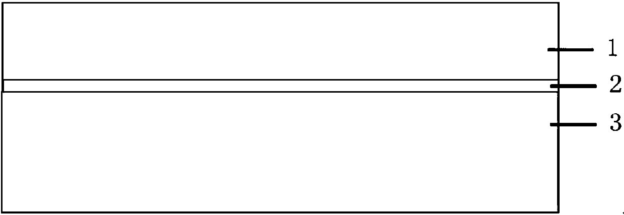
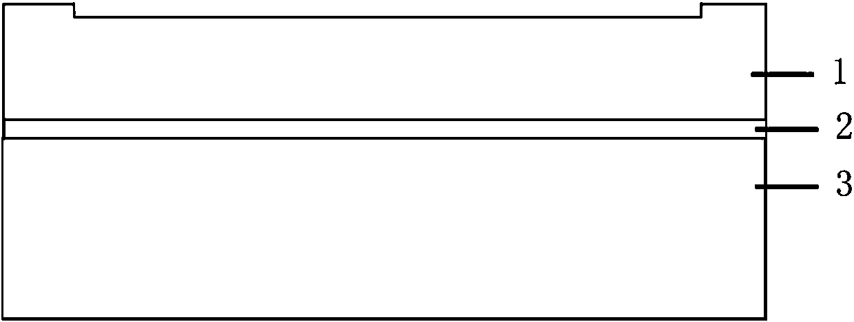
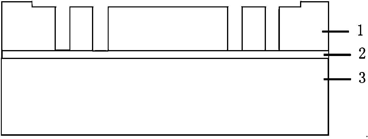
[0025] The raw material is SOI silicon wafer, and the SOI silicon wafer consists of structural layer 1, insulating layer 2 and substrate layer 3 from top to bottom; the thickness of structural layer 1 is 80 μm, N-type silicon, resistivity 0.01~0.1Ω / cm, crystal orientation; the thickness of the insulating layer 2 is 1 μm, and the material is silicon dioxide; the thickness of the substrate layer 3 is 450 μm, and it is N-type silicon.

[0026] The detection capacitance of t...


PUM

PropertyMeasurementUnit
depthaaaaaaaaaa
thicknessaaaaaaaaaa
electrical resistivityaaaaaaaaaa

Abstract

The invention provides a method for machining a multi-capacitor comb micro-accelerometer. The method comprises the following steps: performing shallow slot etching on the surface of a structural layer by means of photoetching; performing photoetching on the surface of the structural layer to define a structural pattern of the micro-accelerometer; etching the structural layer to an insulating layer by adopting deep reactive ion etching (DRIE); corroding the insulating layer by an HF solution; performing photoetching on a glass sheet, corroding glass by a BHF solution, and making a metal electrode and a lead by using a peeling process; bonding the structural layer and the glass sheet; thinning a silicon wafer substrate layer by using a KOH solution; performing photoetching on the surface of the substrate layer, and making a metal electrode by using the peeling process; performing photoetching on the surface of the substrate layer to define the structural pattern of the micro-accelerometer, and etching the substrate layer to the insulating layer by adopting DRIE; and performing splitting, packaging and testing to obtain the required multi-capacitor comb micro-accelerometer. According to the machining method, the detection capacitance area and the masses of mass blocks are increased by the substrate layer, and a produced product has the advantages of high size controllability, simple process, large detection capacitance and capability of meeting the high-accuracy measurement requirement.

Description

technical field [0001] The invention belongs to the technical field of micro-machining of micro-electro-mechanical systems, and in particular relates to a processing method of a multi-capacitance comb-teeth micro-accelerometer. Background technique [0002] In recent years, MEMS technology has developed rapidly, especially micro-accelerometers have been widely used in the field of inertial measurement. From the current international development and application analysis, piezoresistive and capacitive accelerometers are the mainstream of micro accelerometer development. It is generally believed that the piezoresistive type is suitable for the development of micro-accelerometers with low precision, and capacitive accelerometers are generally used for high-precision measurement. There are generally two structures for capacitive micro-accelerometers: "sandwich" structure and "comb tooth" structure. "Sandwich" structure, the quality block can be made very large in both thickness...

Claims


Application Information

Patent Timeline
Patent Type & Authority Patents(China)
IPC IPC(8): B81C1/00G01P15/125
CPCB81C1/00182G01P15/125
Inventor 张照云唐彬苏伟陈颖慧高杨熊壮
Owner INST OF ELECTRONICS ENG CHINA ACAD OF ENG PHYSICS
Why Eureka
Try Eureka